Analog circuit and semiconductor device

a semiconductor and analog circuit technology, applied in the field of analog circuits, can solve the problems of inability to obtain enough dynamic range, circuits formed including thin film transistors with low on/off ratios, and the difference between stoichiometric composition of oxide semiconductors, etc., to achieve wide dynamic range, stable operation, and high sensitivity in detecting signals.

Active Publication Date: 2012-08-14
SEMICON ENERGY LAB CO LTD
View PDF139 Cites 24 Cited by
  • Summary
  • Abstract
  • Description
  • Claims
  • Application Information

AI Technical Summary

Benefits of technology

[0011]In view of the above-described problems, it is an object of an embodiment of the present invention to reduce malfunction of a circuit including a thin film transistor which is formed using an oxide semiconductor.
[0012]Another object of an embodiment of the present invention is to increase the dynamic range of a circuit including a thin film transistor which is formed using an oxide semiconductor.
[0013]Another object of an embodiment of the present invention is to increase sensitivity in detecting signals of a circuit including a thin film transistor which is formed using an oxide semiconductor.
[0014]Another object of an embodiment of the present invention is to reduce power consumption of a circuit including a thin film transistor which is formed using an oxide semiconductor.
[0023]With an embodiment of the present invention, an analog circuit is formed using a thin film transistor in which a purified oxide semiconductor is used, whereby a semiconductor device having a high sensitivity in detecting signals and a wide dynamic range can be obtained.
[0024]By using the thin film transistor in which a highly-purified oxide semiconductor is used, a semiconductor device which operates stably and has low power consumption can be obtained.

Problems solved by technology

However, a difference from the stoichiometric composition in an oxide semiconductor arises in a thin film formation process.
A circuit formed including a thin film transistor with low on / off ratio tends to operate unstably.
In addition, in the case where such a thin film transistor is used in an analog circuit, an enough dynamic range cannot be obtained.
Further, high off-state current causes a problem in that the detection sensitivity to weak signals cannot be increased.
Furthermore, high off-state current also causes a problem of unnecessary current flow, which increases power consumption.

Method used


Image

  • Analog circuit and semiconductor device
  • Analog circuit and semiconductor device
  • Analog circuit and semiconductor device

Examples


embodiment 1

(Embodiment 1)

[0055]A thin film transistor disclosed in this specification in which a purified oxide semiconductor is used can be applied to an analog circuit. As a typical example of the analog circuit, a current mirror circuit can be given, for example. In the case of using a current mirror circuit as a current amplifier circuit, the dynamic range of the current amplifier circuit can be increased, and particularly the sensitivity to a small electric current can be improved.

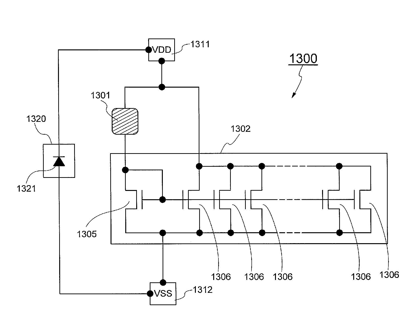
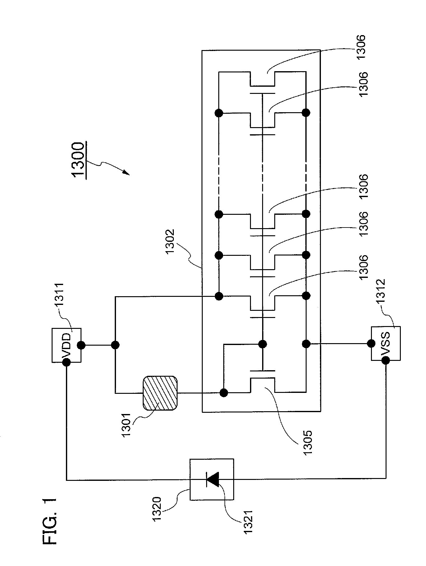
[0056]In this embodiment, a photodetector will be described with reference to FIG. 1 as an example of applying the thin film transistor in which a purified oxide semiconductor is used to a current mirror circuit.

[0057]A photodetector 1300 illustrated in FIG. 1 includes a detector 1301, an amplifier circuit 1302, a power supply terminal 1311 to which a high power supply potential VDD is supplied, a power supply terminal 1312 to which a low power supply potential VSS is supplied, and a protection circuit 1320. In ...

embodiment 2

(Embodiment 2)

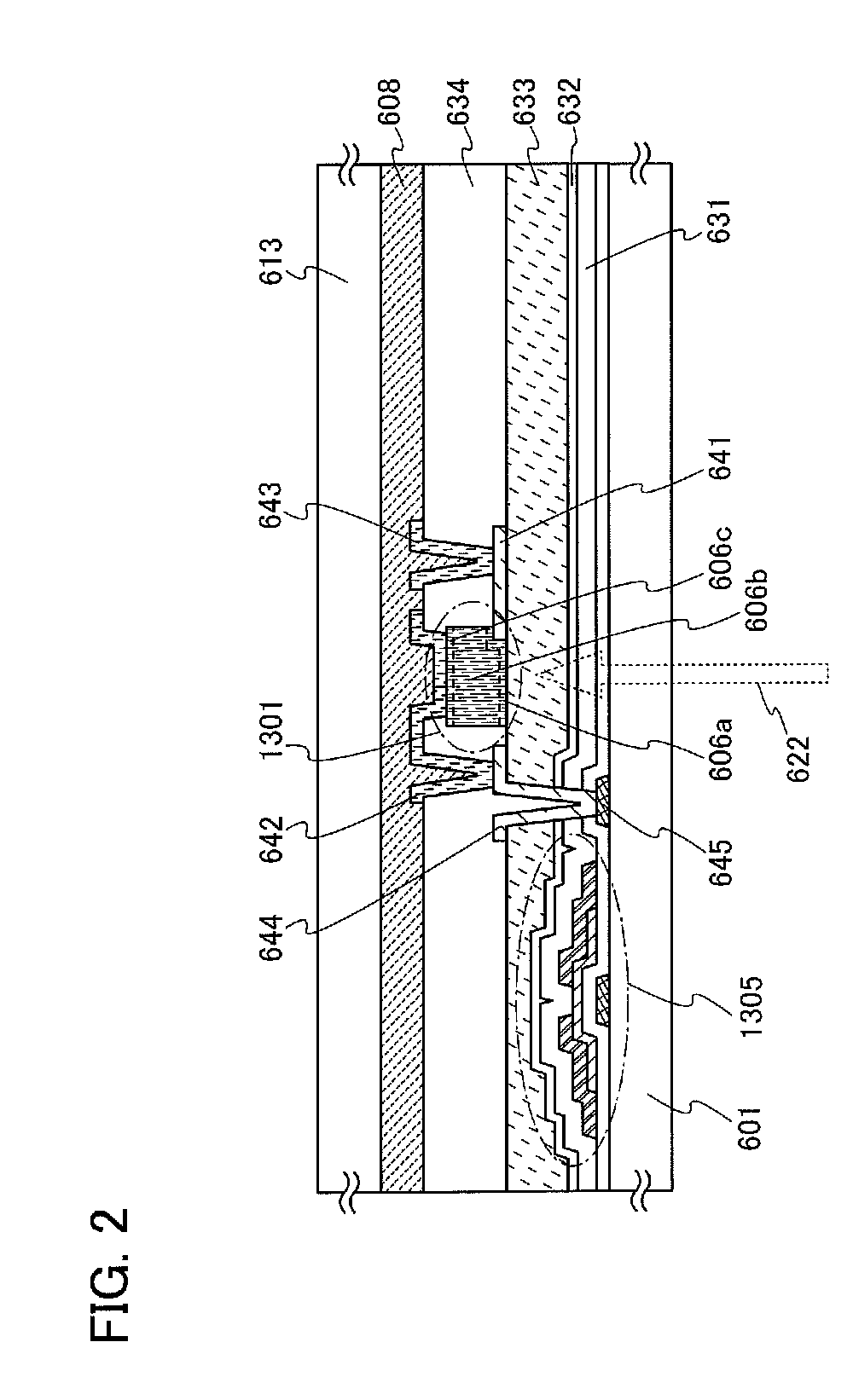
[0073]In this embodiment, an example of a stacked structure of the photodetector 1300 described in Embodiment 1 will be described. An example in which a photodiode is used as the detector 1301 will be described in this embodiment. FIG. 2 is a cross-sectional view illustrating part of the photodetector 1300.

[0074]FIG. 2 is a cross-sectional view illustrating the detector 1301 and the transistor 1305 in the photosensor. The detector 1301 functioning as a sensor and the transistor 1305 are provided over a substrate 601. A substrate 613 is provided over the detector 1301 and the transistor 1305 with an adhesive layer 608 interposed therebetween.

[0075]A substrate used as the substrate 601 needs to have a light-transmitting property and also have such heat resistance as to withstand heat treatment in the manufacturing process. For example, a glass substrate made of aluminosilicate glass, barium borosilicate glass, aluminoborosilicate glass, or the like can be used. Alternati...

embodiment 3

(Embodiment 3)

[0095]In this embodiment, an example of a thin film transistor which is included in the analog circuit described in Embodiment 1 will be described.

[0096]An embodiment of the thin film transistor of this embodiment and a manufacturing method thereof will be described with reference to FIGS. 3A and 3B and FIGS. 4A to 4E.

[0097]An example of a top-surface structure and a cross-sectional structure of the thin film transistor are illustrated in FIGS. 3A and 3B. A thin film transistor 410 illustrated in FIGS. 3A and 3B is a thin film transistor having a top-gate structure.

[0098]FIG. 3A is a top view of the thin film transistor 410 having a top-gate structure, and FIG. 3B is a cross-sectional structure taken along line C1-C2 of FIG. 3A.

[0099]The thin film transistor 410 includes, over a substrate 400 having an insulating surface, an insulating layer 407, an oxide semiconductor layer 412, a source or drain electrode layer 415a, a source or drain electrode layer 4156, a gate ins...


PUM


Abstract

An object is to obtain a semiconductor device having a high sensitivity in detecting signals and a wide dynamic range, using a thin film transistor in which an oxide semiconductor layer is used. An analog circuit is formed with the use of a thin film transistor including an oxide semiconductor which has a function as a channel formation layer, has a hydrogen concentration of 5×10¹⁹ atoms / cm3 or lower, and substantially functions as an insulator in the state where no electric field is generated. Thus, a semiconductor device having a high sensitivity in detecting signals and a wide dynamic range can be obtained.

Description

TECHNICAL FIELD[0001]An embodiment of the present invention relates to an analog circuit including a field effect transistor in which an oxide semiconductor is used. Further, an embodiment of the present invention relates to a semiconductor device including the analog circuit.[0002]In this specification, a semiconductor device means all types of devices which can function by utilizing semiconductor characteristics, and an electrooptic device, a semiconductor circuit, and electric equipment are all semiconductor devices.BACKGROUND ART[0003]A technique for forming a thin film transistor (TFT) by using a semiconductor thin film formed over a substrate having an insulating surface has attracted attention. Thin film transistors are used for display devices typified by a liquid crystal TV set. As a semiconductor thin film that can be applied to the thin film transistors, a silicon-based semiconductor material is known, and as another material, an oxide semiconductor attracts attention.[00...

Claims


Application Information

Patent Timeline
Patent Type & Authority Patents(United States)
IPC IPC(8): H01L25/00
CPCH01L27/1225H01L29/7869H01L33/025H01L29/36H04R1/02H01L21/823412H01L2924/0002H01L2924/00H01L33/00H10K59/351H01L27/124H01L27/1255H01L27/156H01L29/24H01L29/78693H04M1/0266
Inventor YAMAZAKI, SHUNPEIKOYAMA, JUNHIROSE, ATSUSHITSUBUKU, MASASHINODA, KOSEI
Owner SEMICON ENERGY LAB CO LTD
Why Eureka
Try Eureka