CoFe/Ni Multilayer film with perpendicular anistropy for microwave assisted magnetic recording

a multi-layer film, perpendicular anistropy technology, applied in the direction of magnetic bodies, head surfaces, instruments, etc., can solve the problems of inability to integrate devices, all literature examples suffer from at least one drawback, and the use of external magnetic fields generated by current carrying lines to switch the magnetic moment direction becomes problematic, etc., to achieve the effect of improving the robustness of the sil, improving the mr ratio in the spin valve, and improving the robustness

Active Publication Date: 2012-10-30
HEADWAY TECH INC
View PDF5 Cites 28 Cited by
  • Summary
  • Abstract
  • Description
  • Claims
  • Application Information

AI Technical Summary

Benefits of technology

[0011]One objective of the present invention is to improve the robustness of a spin injection layer (SIL) in a MAMR device.
[0016]In still another embodiment, the spin valve structure may be represented by seed layer / [CoFe(t1) / Ni(t2)]X / FeCo / spacer / [CoFe(t1) / Ni(t2)]Y / FeCo / capping layer in a seed / SIL / FeCo / spacer / FGL / FeCo / capping layer configuration. This structure provides the maximum benefit of exchange coupling between a laminated layer with high PMA and a high moment material such as FeCo since easier oscillation is enabled in the FGL simultaneously with improving the robustness of the SIL. Preferably, the FeCo layer that is exchange coupled with the SIL has a thickness less than the SIL and the FeCo layer exchange coupled with the FGL has a thickness between 100 and 300 Angstroms.
[0017]In another aspect, the Cu spacer in the aforementioned CPP-GMR configurations may be modified by inserting a confining current path (CCP) nano-oxide layer (NOL) between upper and lower portions of the Cu spacer. For example, an amorphous oxide such as AlOx with thin metal paths therein may be formed between two copper spacer layers in a Cu / AlOx / Cu configuration. In a CCP-CPP scheme, the Cu metal path is limited through an insulator template so that the MR ratio in the spin valve can be enhanced quite significantly.
[0018]In all embodiments, the substrate may be a main pole layer and a write shield may be formed on the capping layer. The spin valve stack may be annealed between 150° C. and 300° C. for a period of 0.5 to 5 hours. Preferably, the FeCo and Ni layers in the (CoFe / Ni)X laminate are deposited with a very low RF power and a high inert gas pressure to minimize the impinging ion energy so that deposition of a layer does not damage the CoFe or Ni layer on which it is formed. Thus, the interfaces between adjoining CoFe and Ni layers are preserved to maximize the PMA property. Furthermore, this method enables the PMA of (CoFe / Ni)X and (CoFe / Ni)Y laminates to be preserved with a substantially thinner seed layer.

Problems solved by technology

As the size of MRAM cells decreases, the use of external magnetic fields generated by current carrying lines to switch the magnetic moment direction becomes problematic.
As a result, spin valve structures based on PMA are capable of scaling for higher packing density which is a key challenge for future MRAM applications and other spintronic devices.
However, all of the literature examples suffer from at least one drawback.
Unfortunately, FePt or Tb(Fe)Co need high temperature annealing to achieve high enough PMA which is unacceptable for device integration since certain components are damaged by high temperatures.
CoPt and its alloys such as CoCrPt and CoPt—SiO2 are not desirable because Pt and Cr are severe spin depolarizing materials and will seriously quench the amplitude of spintronic devices if incorporated in the spinvalve structures.
As stated above, Co / Pt, Co / Pd, and Co / Ir will not be good PMA materials for spintronic devices because of the severe spin depolarizing property of Pt, Pd, and Ir.
Furthermore, Co / Pt, Co / Pd, and Co / Ir configurations typically require a very thick and expensive Pt, Pd, or Ir as a seed layer.
Au is associated with high cost and easy interdiffusion to adjacent layers which makes a Co / Au multilayer for PMA purposes less practical.
er. The aforementioned seed layers are not practical with Co / Ni multilayer PMA configurations in spintronic devi
ance. Seed layers thicker than about 100 Angstroms will require thinning a different layer in the spin valve to maintain a certain minimum thickness for the spin valve which can easily lead to performance degrad

Method used


Image

  • CoFe/Ni Multilayer film with perpendicular anistropy for microwave assisted magnetic recording
  • CoFe/Ni Multilayer film with perpendicular anistropy for microwave assisted magnetic recording
  • CoFe/Ni Multilayer film with perpendicular anistropy for microwave assisted magnetic recording

Examples


example 1

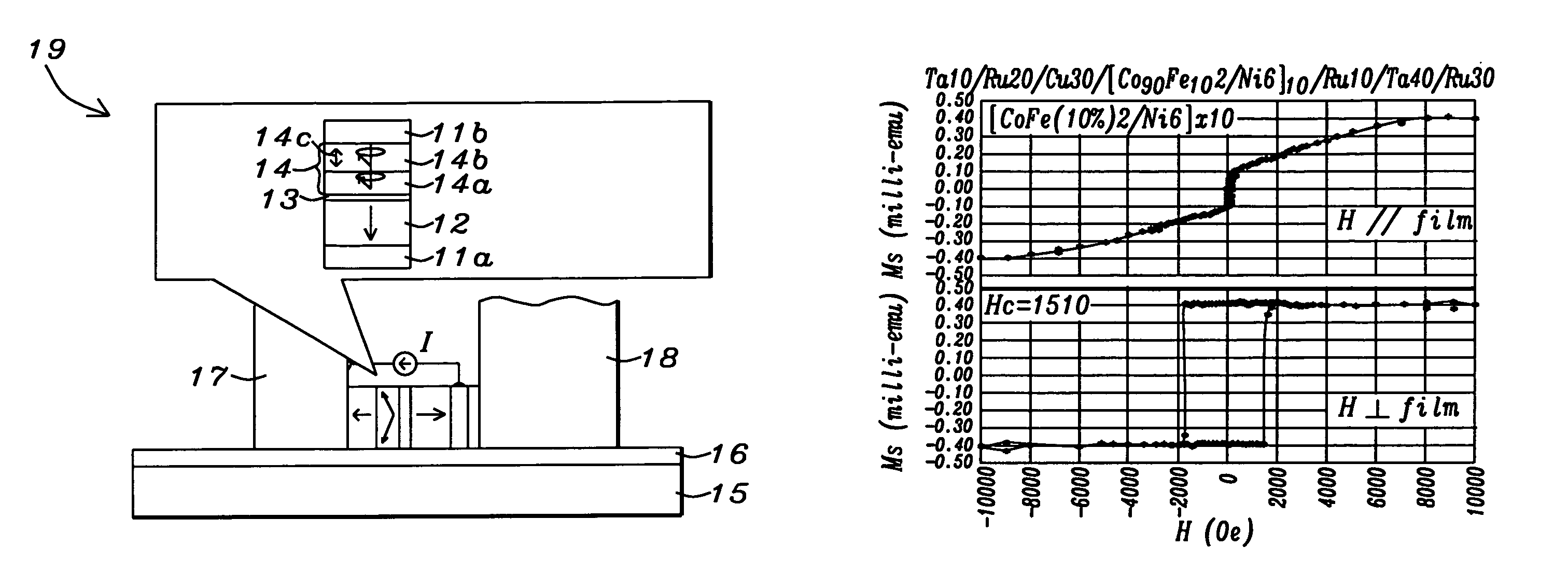
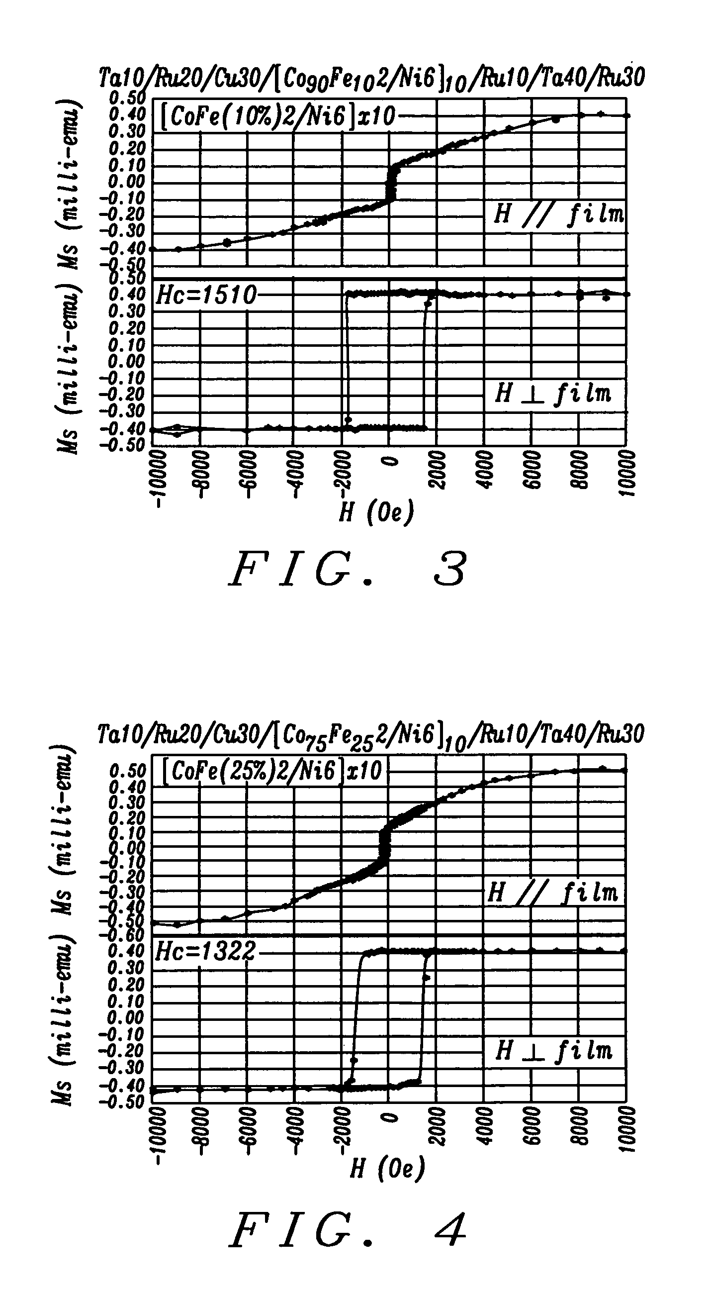
[0060]A series of STO structures comprising a bottom SIL configuration was fabricated to provide examples of the first embodiment. The bottom SIL configuration is represented by Ta10 / Ru20 / Cu20 / [Co(100-Z)FeZ2 / Ni5]X / spacer / FeCo100 / Ru10 / Ta40 / Ru30 where the number following each layer is the thickness in Angstroms. Ta / Ru / Cu is employed as the seed layer, FeCo100 is the FGL, and a (CoFe2 / Ni5)X laminate is the SIL in which each CoFe layer is 2 Angstroms thick and each Ni layer is 5 Angstroms thick and x is maintained between 5 and 50. Fe content in the CoFe laminated layers is kept between 0 and 90 atomic %. A Cu or another metallic spacer is employed for CPP-GMR applications while a AlOx, MgO, TiOx, TiAlOx, MgZnOx, or ZnOx spacer is used for CPP-TMR structures. The capping layer is a Ru10 / Ta40 / Ru30 composite. Based on torque measurements, we deduced that Hk for each (CoFe / Ni)X stack is >15000 Oersted (Oe).

example 2

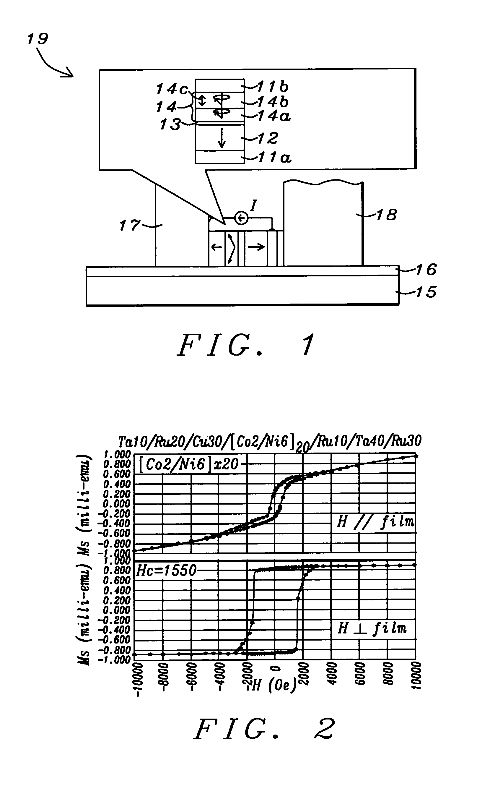
[0061]A preferred bottom SIL configuration was fabricated and is represented by Ta10 / Ru20 / Cu20 / [Co100-Z)FeZ2 / Ni5]X / spacer / [Co(100-Z)FeZ2 / Ni5]Y / FeCo100 / Ru10 / Ta40 / Ru30. This structure is a modification of the first embodiment where a (CoFe / Ni)Y laminate is inserted between the non-metallic spacer and the FeCo100 layer to give a composite FGL where y is between 5 and 30. Since the [Co(100-Z)FeZ2 / Ni5]Y laminate has a strong magnetic coupling with the FeCo100 layer, the large PMA of the [Co(100-Z)FeZ2 / Ni5]Y laminate will force the anisotropy of the FeCo to tilt partially toward the perpendicular to plane direction so that the entire FGL can easily oscillate under a low current density.

example 3

[0062]A series of STO structures comprising a top SIL configuration was fabricated according to another embodiment of the present invention. The top SIL configuration is represented by Ta10 / Ru20 / Cu20 / FeCo100 / spacer / [Co(100-Z)FeZ2 / Ni5]X / Ru10 / Ta40 / Ru30 where the number following each layer is the thickness in Angstroms. Ta / Ru / Cu is employed as the seed layer, FeCo100 is the FGL, and a (CoFe2 / Ni5)X laminate is the SIL in which each CoFe layer is 2 Angstroms thick and each Ni layer is 5 Angstroms thick and x is maintained between 5 and 50. Fe content in the CoFe laminated layers is kept between 0 and 90 atomic %. Cu or another metallic spacer is employed for CPP-GMR embodiments while a AlOx, MgO, TiOx, TiAlOx, MgZnOx, or ZnOx spacer is used for CPP-TMR structures. The capping layer is a Ru10 / Ta40 / Ru30 composite. Based on torque measurements, we deduced that Hk for each (CoFe / Ni)X stack is >15000 Oersted (Oe).


PUM

PropertyMeasurementUnit
thicknessaaaaaaaaaa
thicknessaaaaaaaaaa
thicknessaaaaaaaaaa

Abstract

A spin transfer oscillator with a seed / SIL / spacer / FGL / capping configuration is disclosed with a composite seed layer made of Ta and a metal layer having a fcc(111) or hcp(001) texture to enhance perpendicular magnetic anisotropy (PMA) in an overlying (A1 / A2)X laminated spin injection layer (SIL). Field generation layer (FGL) is made of a high Bs material such FeCo. Alternatively, the STO has a seed / FGL / spacer / SIL / capping configuration. The SIL may include a FeCo layer that is exchanged coupled with the (A1 / A2)X laminate (x is 5 to 50) to improve robustness. The FGL may include an (A1 / A2)Y laminate (y=5 to 30) exchange coupled with the high Bs layer to enable easier oscillations. A1 may be one of Co, CoFe, or CoFeR where R is a metal, and A2 is one of Ni, NiCo, or NiFe. The STO may be formed between a main pole and trailing shield in a write head.

Description

RELATED PATENT APPLICATIONS[0001]This application is related to the following: Ser. No. 12 / 456,621, filing date Jun. 19, 2009; and Ser. No. 12 / 589,614, filing date Oct. 26, 2009; assigned to the same assignee and herein incorporated by reference in their entirety.FIELD OF THE INVENTION[0002]The invention relates to a high performance spin valve in which (CoFe / Ni)n multi-layer structures having high perpendicular magnetic anisotropy (PMA) are used to establish partial PMA in high moment materials such as FeCo through exchange coupling thereby enabling easier flux generation layer (FGL) oscillations in microwave assisted magnetic recording (MAMR).BACKGROUND OF THE INVENTION[0003]Magnetoresistive Random Access Memory (MRAM), based on the integration of silicon CMOS with MTJ technology, is a major emerging technology that is highly competitive with existing semiconductor memories such as SRAM, DRAM, and Flash. Similarly, spin-transfer (spin torque or STT) magnetization switching describ...

Claims


Application Information

Patent Timeline
Patent Type & Authority Patents(United States)
IPC IPC(8): G11B5/235G11B5/31G11B5/39
CPCB82Y10/00G01R33/093G01R33/1284G11B5/1278G11B5/3153G11B5/3909H01F10/3286H01F41/305H01F10/329H01L43/08H01L43/10H01L43/12B82Y40/00H01F10/3295H01F10/3259B82Y25/00Y10T428/1121G11B5/3967G11B2005/0024G11B2005/3996H01F10/325H01F10/3254Y10T428/1129Y10T428/1114H01F1/0579Y10T428/115G11B5/33G11C11/1673G11C11/1675G11C11/18G11C11/161H10N50/10H10N50/01H10N50/85G11B5/235H10B61/00H10N50/80
Inventor ZHANG, KUNLIANGLI, MINZHOU, YUCHEN
Owner HEADWAY TECH INC
Why Eureka
Try Eureka