Insulating thin film, formation solution for insulating thin film, field-effect transistor, method for manufacturing the same and image display unit

a technology of formation solution and insulating thin film, which is applied in the direction of thermoelectric devices, solid-state devices, radiation controlled devices, etc., can solve the problems of insufficient fet properties of insulating layers, inability to obtain insulating properties in sufficient quantities, and inability to produce fet properties

Active Publication Date: 2012-11-13
TOPPAN PRINTING CO LTD
View PDF11 Cites 3 Cited by
  • Summary
  • Abstract
  • Description
  • Claims
  • Application Information

AI Technical Summary

Problems solved by technology

However, the gate insulating layer frequently has insufficient FET properties, because the gate insulating layer generally has low relative permittivity of approximately 2.5-3.8.
However, there is a problem in a use of the organic-inorganic hybrid material.
Hence, insulating properties cannot be sufficiently obtained, because the thin film is influenced by acid or base which remains inside of the film.
Thus, it led to a new problem such as an occurrence of a high leak current.
Thus, FET properties become poorly-reproducible.
However, in return for the stabilization, the organic-inorganic hybrid material or the organic-inorganic composite material requires a relatively high temperature baking because of its poor reactivity.
Further, after the thin film is formed, since the materials have a weak tolerance for a post-processing such as a surface processing for the insulating thin film, FET properties has been made poor because of change in a shape of the surface or chemical properties caused by the hard processing.
Therefore, there is a problem that materials for the electrode, the insulator and the semiconductor formed on a substrate are separated from the substrate by the developing solution or etchant.
In particular, when a plastic film is used as a substrate, adhesion between the plastic and the metal or the metal oxide is not sufficient.
Thus, this problem is remarkable.

Method used


Image

  • Insulating thin film, formation solution for insulating thin film, field-effect transistor, method for manufacturing the same and image display unit
  • Insulating thin film, formation solution for insulating thin film, field-effect transistor, method for manufacturing the same and image display unit
  • Insulating thin film, formation solution for insulating thin film, field-effect transistor, method for manufacturing the same and image display unit

Examples


example 1

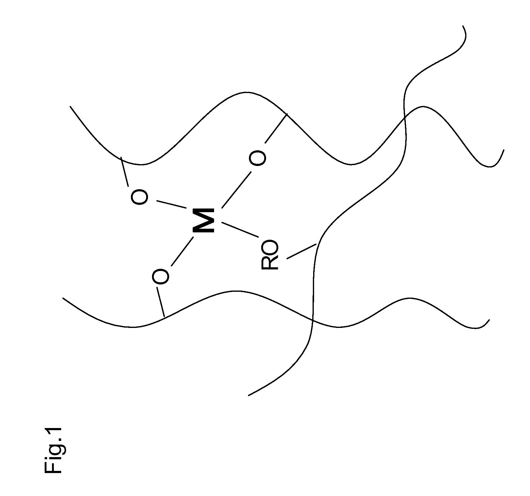
[0091]1 g of Tetra-n-butyl titanate ((nBuO)4Ti) as a metallic compound, 1.5 g of polyvinyl phenol (PVP) as a polymer compound and 2 g of methylolmelamine as an organic molecule were respectively solved in n-butanol, toluene / n-butanol and toluene / n-butanol. Moreover, the above materials were mixed by dipping carefully while they were stirred under an Ar atmosphere. Thus, an orange colored solvent was obtained. Furthermore, the formation solution for the insulating thin film was obtained as a transparent orange colored solvent by putting the obtained orange colored solvent through a PTFE filter with pore sizes of 0.2 μm.

[0092]2 ml of the formation solution for the insulating thin film was spin coated on a glass substrate, dried at 90 degrees Celsius for 10 minutes and baked at 120 degrees Celsius for 1 hour. Thus, the insulating thin film with a thickness of 800 nm was obtained.

[0093]The obtained insulating thin film was analyzed by XPS. The inside of the insulating thin film was anal...
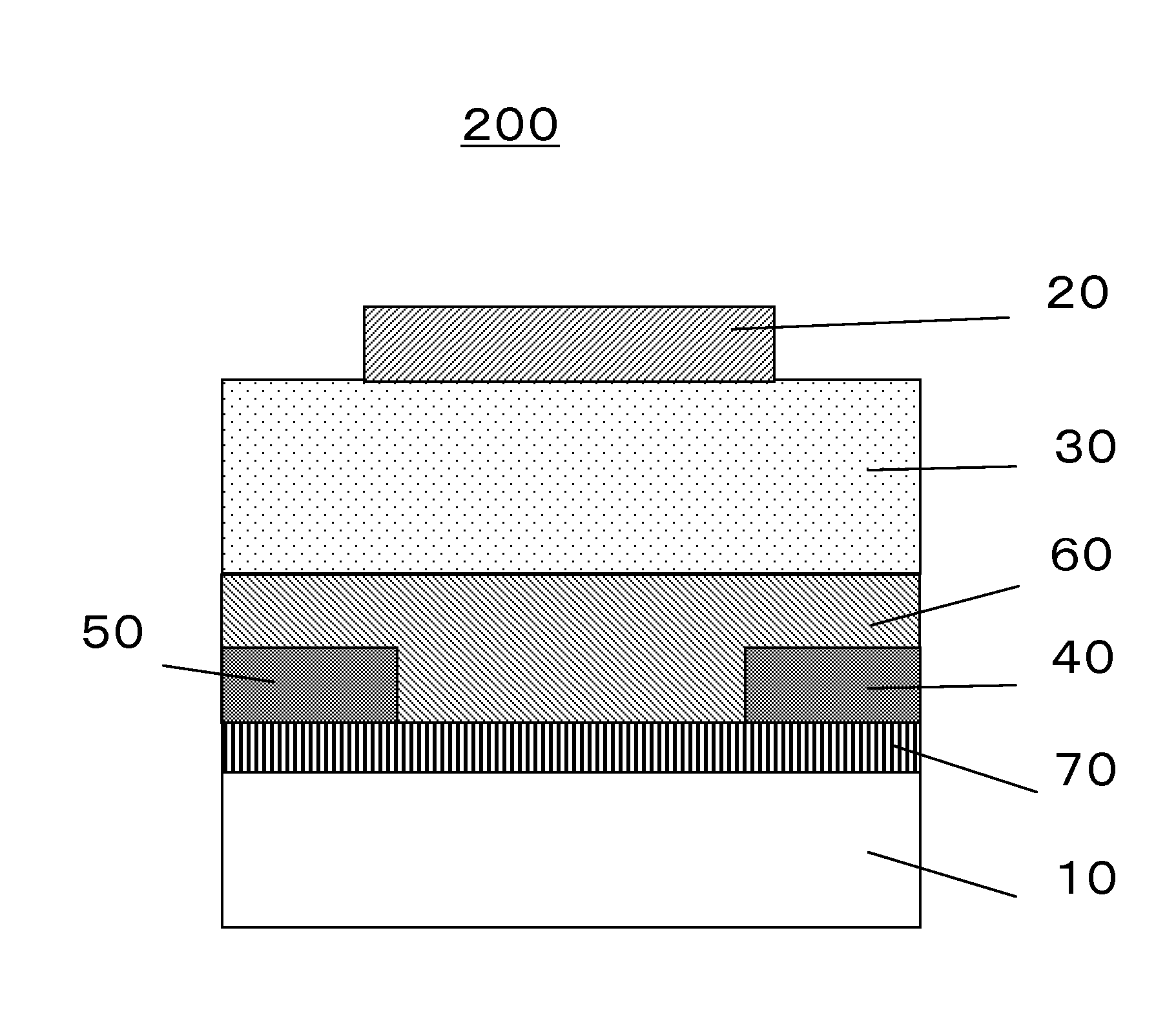
example 2

[0096]A self-assembled monolayer 31 made of octadecyltrichlorosilane (OTS) was formed on the surface of the insulating thin film obtained in Example 1. First, the surface processing was performed for 5 minutes on the insulating thin film of Example 1 using a UV / ozone irradiation device and the surface had hydrophilic properties. The obtained contact angle of pure water on the surface was 5.4°. Furthermore, the insulating thin film having hydrophilic properties on its surface was dipped for one night in a dry toluene solvent of OTS. Thus, the self-assembled monolayer 31 was obtained. The contact angle of pure water of the surface of the obtained self-assembled monolayer 31 was 103°. The surface was observed using AFM (Atomic Force Microscope), then, a coverage of OTS was 100%.

example 3

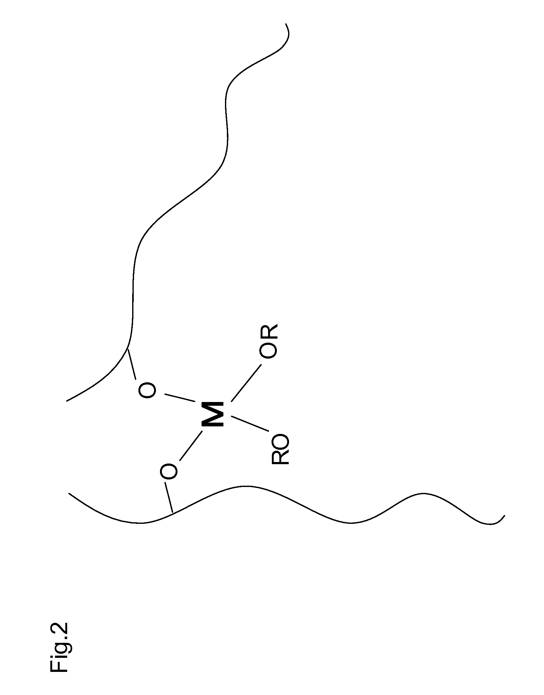
[0097]1 g of a solvent having diisopropoxybis titanium (triethanolaminato) at 80% as a metallic compound, 1 g of polyvinyl alcohol (PVA) as a polymer compound and 2 g of 3-amino-1,2,4-triazole as an organic molecule were respectively solved in water. Moreover, the above materials were mixed by dipping carefully while they were stirred under an Ar atmosphere. Thus, a colorless solvent was obtained. Furthermore, the formation solution for the insulating thin film was obtained as a transparent solvent by putting the obtained colorless solvent through a PTFE filter with pore sizes of 0.2 μm.

[0098]2 ml of the obtained formation solution for the insulating thin film was spin coated on a glass substrate, dried at 90 degrees Celsius for 10 minutes and baked at 150 degrees Celsius for 1 hour. Thus, the insulating thin film with a thickness of 1000 nm was obtained.

[0099]The obtained insulating thin film was analyzed by XPS. The inside of the insulating thin film was analyzed by etching for 10...


PUM

PropertyMeasurementUnit
relative permittivityaaaaaaaaaa
temperatureaaaaaaaaaa

Abstract

One embodiment of the present invention is an insulating thin film having a polymer compound, a metallic atom bonded to the polymer compound through an oxide atom and selected from a group 4 element, a group 5 element, a group 6 element, a group 13 element, zinc or tin, and an organic molecule bonded to the metallic atom through the oxide atom or a nitrogen atom.

Description

CROSS REFERENCE TO RELATED APPLICATION[0001]This application is based on and claims the benefit of priority from the Japanese Patent Application number 2009-115547, filed on May 12, 2009 and the Japanese Patent Application number 2009-127561, filed on May 27, 2009; the entire contents of which are incorporated herein by reference.BACKGROUND OF THE INVENTION[0002]1. Field of the Invention[0003]The present invention relates to an insulating thin film, a formation solution for the insulating thin film, a method for manufacturing the insulating thin film, a field-effect transistor, a method for manufacturing the field-effect transistor and an image display unit. Particularly, the present invention relates to the insulating thin film having high insulating properties and high electric permittivity, the formation solution for the insulating thin film, the method for manufacturing the insulating thin film, the field-effect transistor, the method for manufacturing the field-effect transisto...

Claims


Application Information

Patent Timeline
Patent Type & Authority Patents(United States)
IPC IPC(8): H01L29/08
CPCH01L29/4908H01L29/7869
Inventor ITO, YUTAKA
Owner TOPPAN PRINTING CO LTD
Why Eureka
Try Eureka