Light emitting device

a light emitting device and light technology, applied in the direction of semiconductor devices, basic electric elements, electrical equipment, etc., can solve the problems of low efficiency as light emitting devices, low light emitting efficiency, low efficiency, etc., to achieve high efficiency, improve light emitting efficiency, and facilitate the effect of carrying ou

Inactive Publication Date: 2012-11-13
PANASONIC CORP
View PDF19 Cites 3 Cited by
  • Summary
  • Abstract
  • Description
  • Claims
  • Application Information

AI Technical Summary

Benefits of technology

[0010]Therefore, an object of the present invention is to provide a light emitting device that can improve the light emitting efficiency of phosphor particles, and easily provide a large-area device with high light emitting efficiency.
[0026]In accordance with the light emitting device of the present invention, since the n-type nitride semiconductor portion and the p-type nitride semiconductor portion are included in a single phosphor particle, light emission is easily carried out by a combination of an electron and a hole so that the light emitting efficiency can be improved.
[0027]Moreover, in each single phosphor particle, the n-type nitride semiconductor portion and the p-type nitride semiconductor portion have the common c-axe in the respective crystal structures, that is, c-axe of the n-type nitride semiconductor portion and c-axe of the p-type nitride semiconductor portion is made in parallel with each other, with the n-type nitride semiconductor portion and the p-type nitride semiconductor portion being made in contact with each other on a plane in parallel with the c-axe. For this reason, all the electric current paths inside the phosphor particle can be aligned in a direction perpendicular to the c-axis so that light emission with high efficiency can be obtained; thus, it becomes possible to obtain a light emitting device with high light emitting efficiency.
[0028]Furthermore, the phosphor particle may be formed by processes in which an insulating film is formed on the n-type nitride semiconductor portion, and one portion of the insulating film is removed so as to allow a plane in parallel with the c-axis of the n-type nitride semiconductor portion to be exposed so that the p-type nitride semiconductor portion is grown on the exposed n-type nitride semiconductor portion. Alternatively, an insulating film may be formed on the p-type nitride semiconductor portion, and one portion of the insulating film may be removed so as to allow a plane in parallel with the c-axis of the p-type nitride semiconductor portion to be exposed so that the n-type nitride semiconductor portion is grown thereon. With this structure, the epitaxial surface and the nitride semiconductor portion to be grown thereon can be prepared as nitride semiconductors having the same wurtzite crystal structure so that it becomes possible to suppress strains and dislocations that tend to occur upon epitaxial growth, and consequently to improve the light emitting efficiency of the phosphor particle.
[0029]Moreover, each phosphor particle may be designed so as to satisfy an expression (particle length along the common c-axis) / (minimum width on bottom face perpendicular to c-axis)≧2; thus, the side faces of each phosphor particle can be easily brought into contact with either one of the electrodes so that light emission luminance can be enhanced.

Problems solved by technology

However, even in the case where an electric field light emitting device is formed by using the phosphor particles in accordance with the prior art described in Japanese Patent Laid-open Publication No. 2006-117735, a problem arises in which its light emitting efficiency is low.
The other is that, since the electric current path inside the phosphor is not defined in the prior art, two electric current paths, that is, an electric current path having low light emitting efficiency and an electric current path having high light emitting efficiency, are mixedly present, with the result that the efficiency as a light emitting device becomes low.
This is because, in the case where the electric current path is in parallel with the c-axis direction, part of energy for use in emitting light is unnecessarily consumed due to influences of the polarity.

Method used


Image

  • Light emitting device
  • Light emitting device
  • Light emitting device

Examples


first embodiment

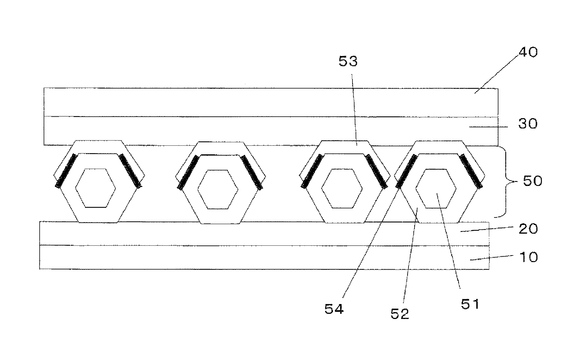
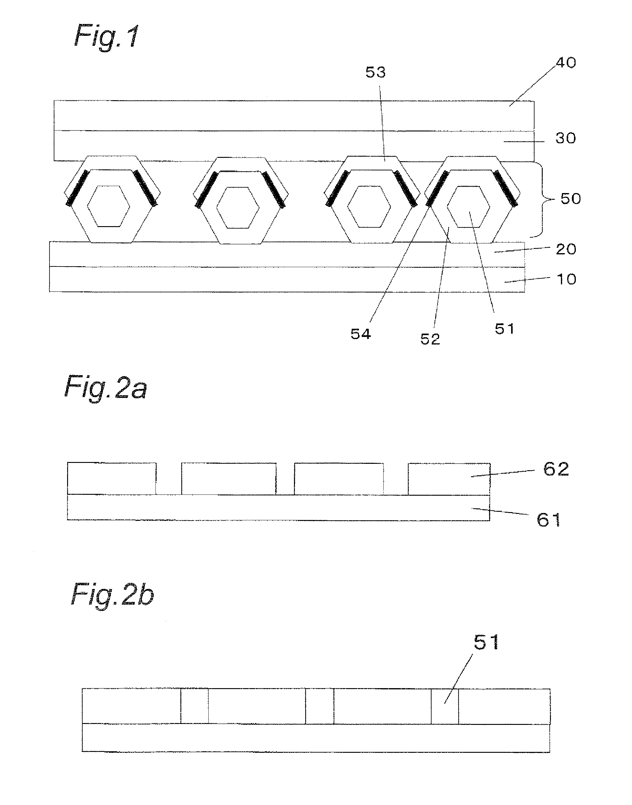
[0062]FIG. 1 shows a schematic structure of a light emitting device in accordance with first embodiment of the present invention. This light emitting device has a structure in which a lower electrode 20, phosphor particles 50, an upper electrode 30 and an upper substrate 40 that are placed on a lower substrate 10 in this order. Additionally, FIG. 1 shows a minimum structure for use in emitting light, and other members may be further included thereon.

[0063]In this light emitting device, since an n-type nitride semiconductor portion 52 and a p-type nitride semiconductor portion 53 are placed inside one phosphor particle 50, light is easily emitted by a combination of an electron and a hole so that the light emitting efficiency is improved. Moreover, in each single phosphor particle 50, the n-type nitride semiconductor portion 52 and the p-type nitride semiconductor portion 53 are aligned, with c-axe of the respective crystal structures being in parallel with each other, and the n-type...

example 1

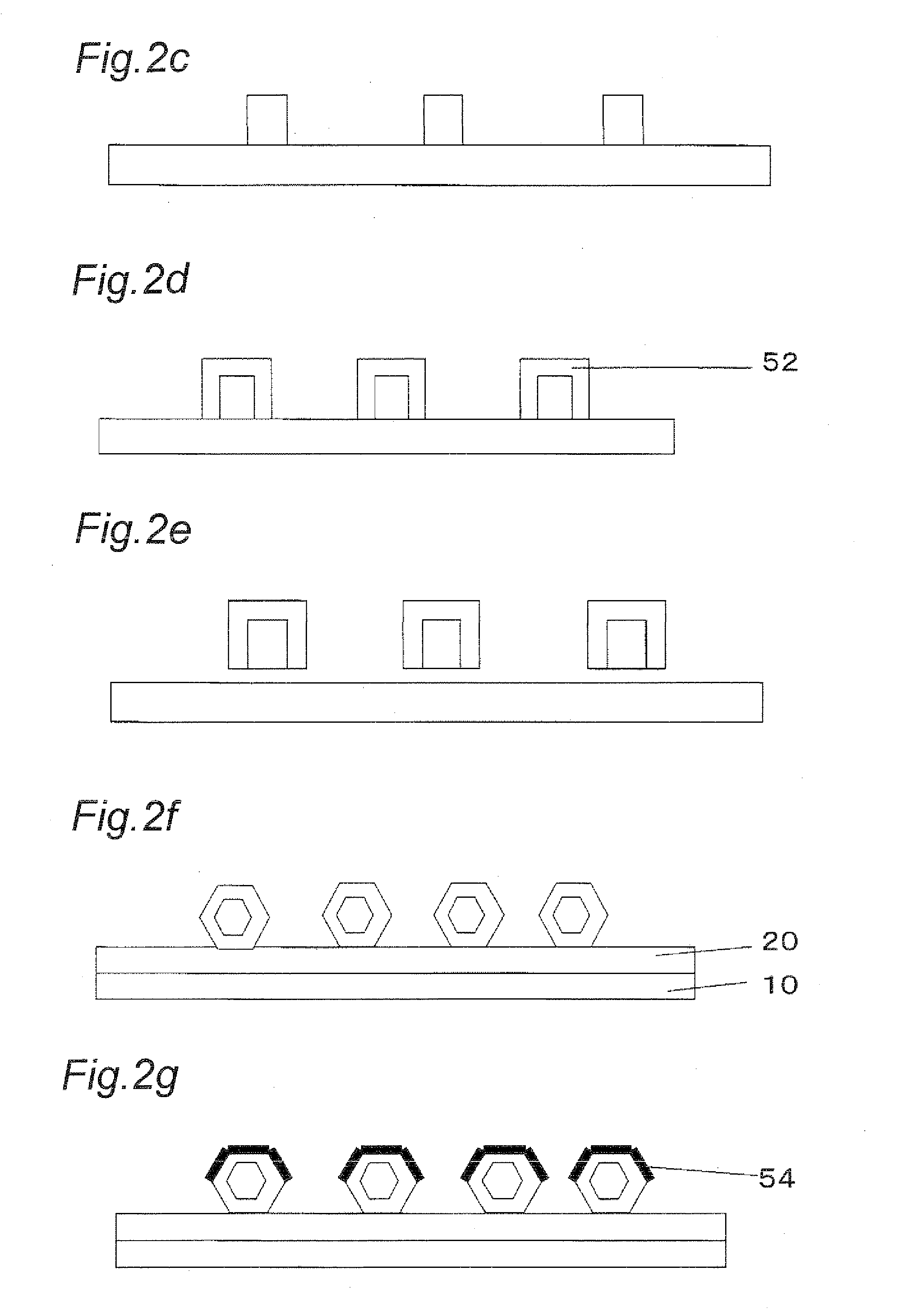
[0076]In the following, a method for manufacturing a light emitting device in accordance with example 1 will be described.

[0077](a) A sapphire substrate of 2 inches (5.08 cm) having a plane orientation (0, 0, 0, 1) was used as an epitaxial substrate. On the sapphire substrate, an SiO2 film having a thickness of 10 μm was formed by using a sputtering method, with a formation mask being interposed therebetween. The diameter of each pore portion was 2 μm. An SiO2 target was used as the target, and the sputtering was carried out in an Ar gas atmosphere so as to form the film.

(b) An AlN film was formed thereon by sputtering as a nucleus film. An Al target was used as the target, and the sputtering was carried out in an N2 gas atmosphere so as to form the film. The AlN was grown in the c-axis direction, with a thickness of 10 μm.

(c) The epitaxial substrate on which an epitaxial mask and nuclei had been formed was immersed in a 3% aqueous hydrofluoric acid solution so that the epitaxial ma...

example 2

[0083]In example 2, the same method as that of example 1 was carried out except that no insulating film for phosphor particles was formed so that a light emitting device was obtained.

[0084]When a voltage was applied to the resulting light emitting device in the same manner as in example 1 so as to emit light, its luminance was 520 cd / m2, and its light emitting efficiency was 1.1 lm / W.


PUM


Abstract

A light emitting device is provided with: a pair of an anode and a cathode that are opposed to each other; and a phosphor layer, composed of a plurality of phosphor particles, that is sandwiched between the paired anode and cathode, from direction that is perpendicular to main surfaces of the anode and the cathode, and in this structure, each phosphor particle is a nitride semiconductor phosphor particle having a wurtzite crystal structure that contains an n-type nitride semiconductor portion and a p-type nitride semiconductor portion, with the n-type nitride semiconductor portion being made in contact with the cathode and the p-type nitride semiconductor portion being made in contact with the anode, and the n-type nitride semiconductor portion and the p-type nitride semiconductor portion have the common c-axe in the respective crystal structures thereof made in parallel with each other, with the n-type nitride semiconductor portion and the p-type nitride semiconductor portion being made in contact with each other on a plane in parallel with the c-axe.

Description

RELATED APPLICATIONS[0001]This application is the U.S. National Phase under 35 U.S.C. §371 of International Application No. PCT / JP2009 / 000787, filed on Feb. 24, 2009, which in turn claims the benefit of Japanese Application No. 2008-221271, filed on Aug. 29, 2008, the disclosures of which Applications are incorporated by reference herein.BACKGROUND[0002]1. Technical Field[0003]The present invention relates to an electric field light emitting device of a direct current driving type in which nitride semiconductor phosphor particles having a wurtzite crystal structure are used.[0004]2. Background Art[0005]Among light emitting devices operated by a direct electric current, as practicable semiconductor materials to be used for light emitting devices, such as a blue light-emitting diode (Blue-LED) and an ultra-violet light emitting diode (UV-LED), in particular, GaN-based semiconductors typified by gallium nitride (GaN), indium nitride-gallium mixed crystal (InGaN), aluminum nitride-galli...

Claims


Application Information

Patent Timeline
Patent Type & Authority Patents(United States)
IPC IPC(8): H01L33/32
CPCH01L33/18H01L33/24
Inventor SHIMAMURA, TAKAYUKIONO, MASAYUKITANIGUCHI, REIKOSATOH, EIICHIODAGIRI, MASARU
Owner PANASONIC CORP
Why Eureka
Try Eureka