Spin-polarized electron source

a spin-polarized electron source and spin-polarized technology, applied in the direction of discharge tube/lamp details, discharge tube main electrodes, electric discharge lamps, etc., can solve the problem of low polarization and structure, and achieve high polarization, reduce the dislocation density of the strained superlattice layer on the buffer layer, and improve external quantum efficiency

Active Publication Date: 2013-01-01
JAPAN SCI & TECH CORP
View PDF14 Cites 0 Cited by
  • Summary
  • Abstract
  • Description
  • Claims
  • Application Information

AI Technical Summary

Benefits of technology

[0032]According to the present invention, since the intermediate layer formed of a crystal having a lattice constant greater than that of a crystal of the buffer layer is provided beneath the buffer layer, tensile strain can be imposed on the buffer layer, whereby dislocation density of the strained superlattice layer on the buffer layer can be reduced. As a result, the spin-flip scattering of excited electrons caused by dislocations and the capture of electrons by dislocations reduce, so that spin polarization of electrons excited in the conduction band of the strained superlattice layer can be increased, and external quantum efficiency can be improved. That is, regardless of the choice of the materials of the buffer layer and the substrate, tensile strain can be imposed on the buffer layer, thereby enabling provision of high polarization and high quantum efficiency through improvement of crystallinity of the strained superlattice layer.

Problems solved by technology

However, the structure is fails to provide high polarization.Patent Document 1: Japanese Patent No. 3189444Patent Document 2: Japanese Patent Application Laid-Open (kokai) No.

Method used


Image

  • Spin-polarized electron source
  • Spin-polarized electron source
  • Spin-polarized electron source

Examples


example 1

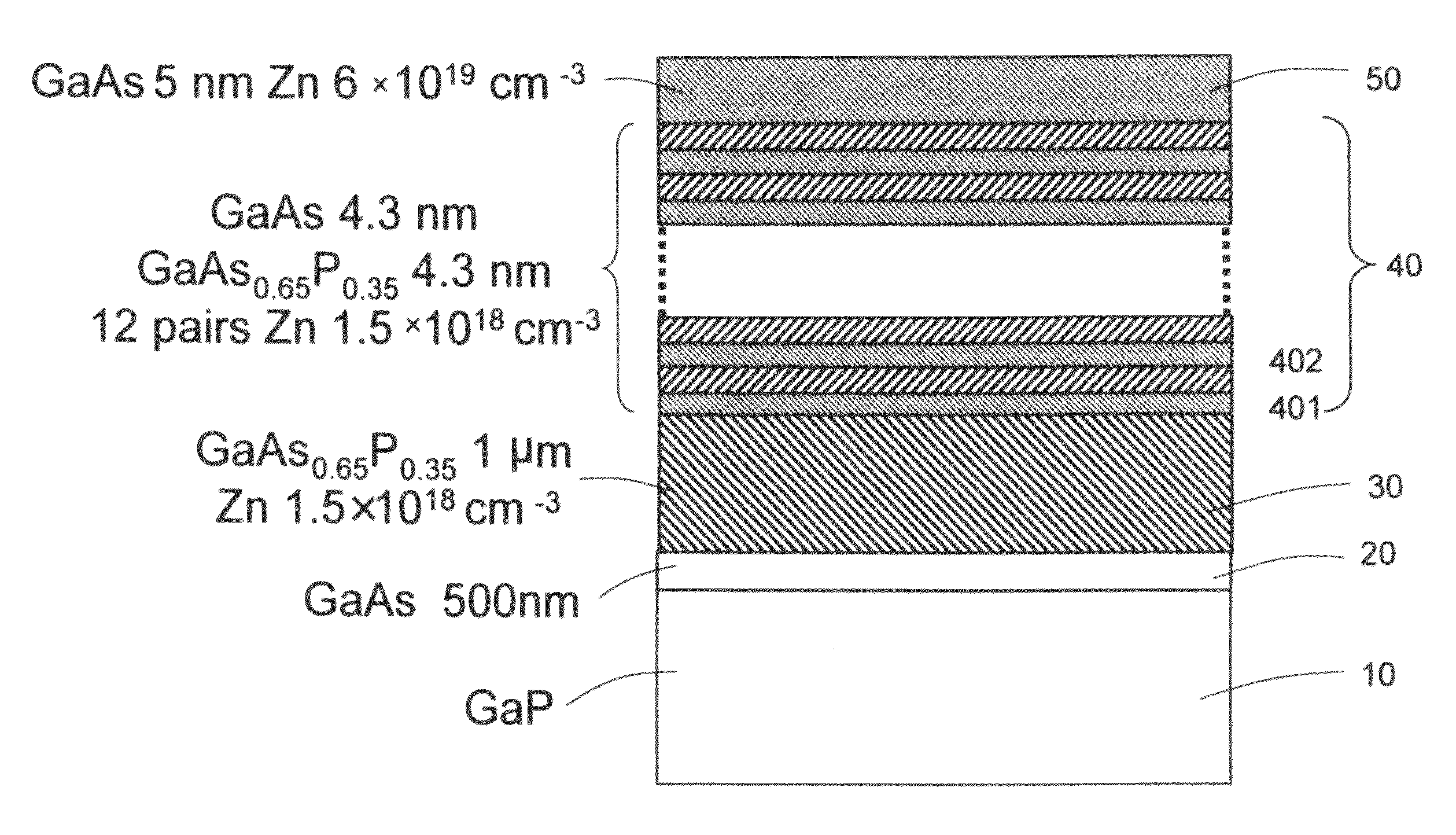
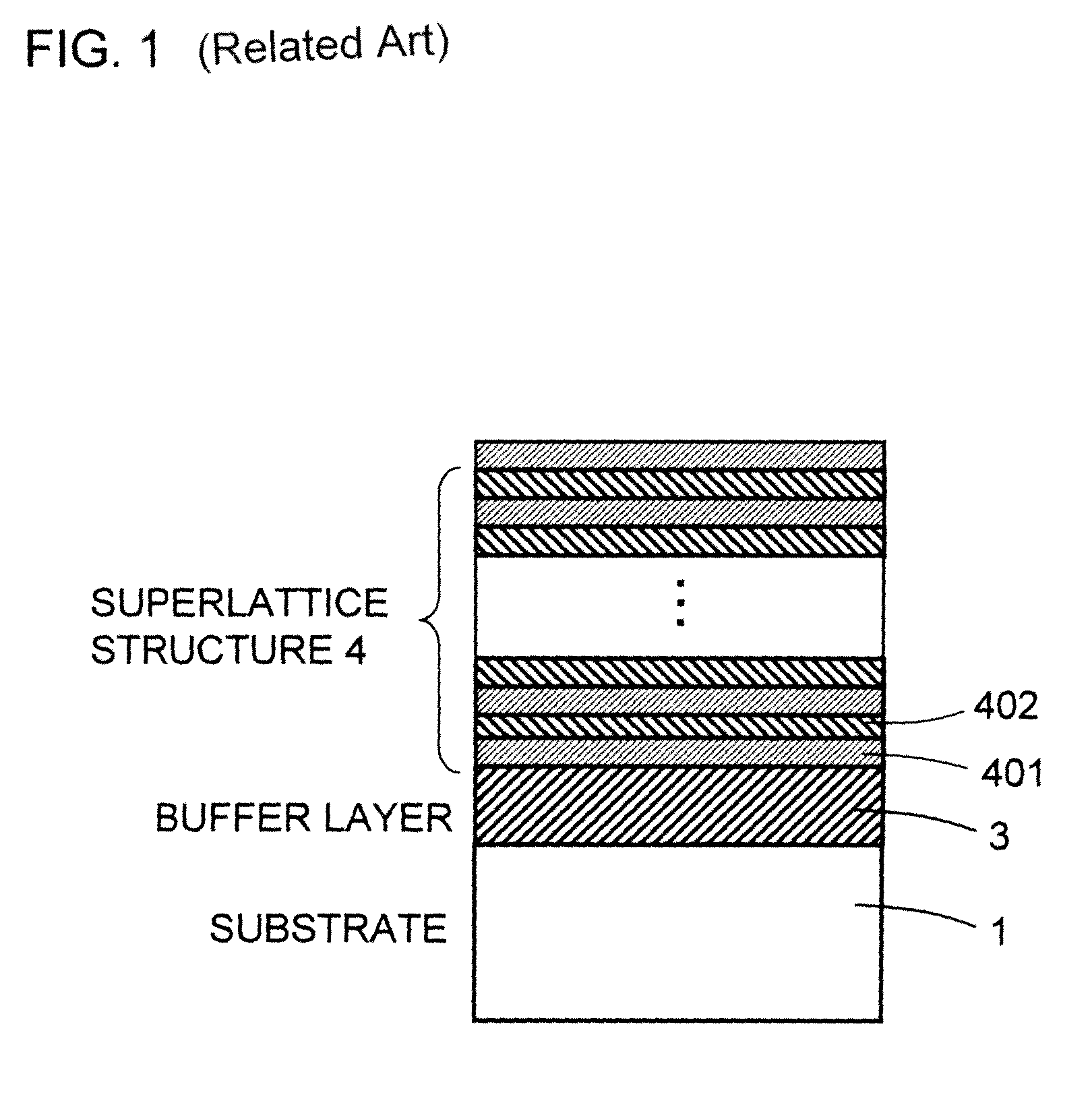
[0089]As shown in FIG. 4, Example 1 is a spin-polarized electron generating device which uses a GaP substrate and a GaAsP / GaAs strained superlattice layer. Specifically, an intermediate layer 20 formed of GaAs having a thickness of 500 nm is formed on a substrate 10 formed of GaP; a buffer layer 30 having a thickness of 1 μm is formed on the intermediate layer 20; a strained superlattice layer 40 is formed on the buffer layer 30; and a cap layer 50 having a thickness of 5 nm is formed on the strained superlattice layer 40.

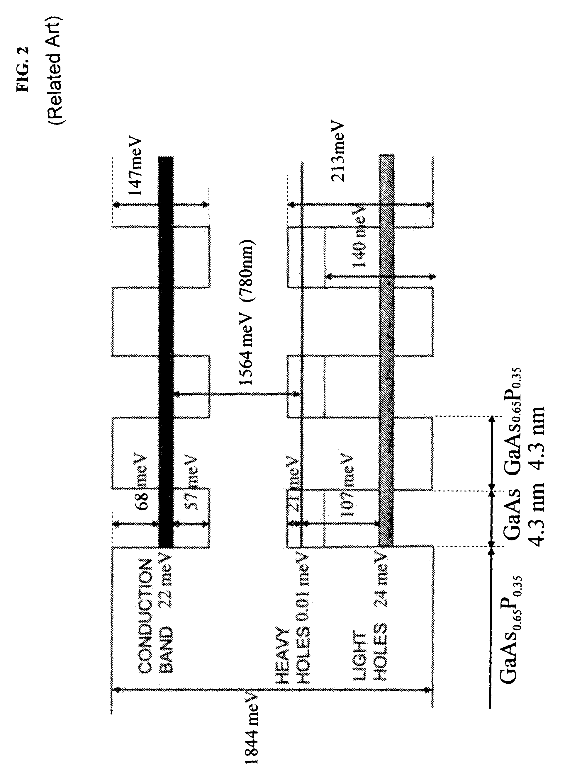
[0090]This structure is a transmission-type strained superlattice semiconductor photocathode designed for use as a spin-polarized electron generating device of high polarization and high brightness. The strained superlattice layer 40 was designed as shown in FIG. 4 on the basis of theoretical calculation. Specifically, the buffer layer 30 is formed of GaAs0.65P0.35 having a thickness of 1 μm and doped with Zn at a concentration of 1.5×1018 cm−3. The strained superl...

example 2

[0095]As shown in FIG. 7, Example 2 is a spin-polarized electron generating device which uses a GaAs substrate and a GaInP / GaInAs strained superlattice layer. For a certain purpose of use of an electron generating device, it is necessary to increase current which can be extracted from a photocathode. One method to increase current to be extracted is to increase power of excitation light. In application to an electron microscope or a like application, utilization of a small-sized, highly versatile semiconductor laser, rather than a large-sized laser, is effective. Many versatile semiconductor lasers having an emission wavelength of 900 nm to 1,000 nm and an output of several W are available. Therefore, utilization of a strained superlattice in which electrons are excited by excitation light in this wavelength range is effective. Also, for reduction of size, use of a transmission type is indispensable.

[0096]As shown in FIG. 7, the spin-polarized electron generating device of the prese...

example 3

[0100]As shown in FIG. 8, Example 3 is a spin-polarized electron generating device which uses a GaN substrate and a GaN / GaInN strained superlattice layer. As shown in FIG. 8, the spin-polarized electron generating device of the present example is configured as follows: an intermediate layer 22 formed of InN having a thickness of 500 nm is formed on a substrate 12 formed of GaN; a buffer layer 32 having a thickness of 1 μm is formed on the intermediate layer 22; a strained superlattice layer 42 is formed on the buffer layer 32; and a cap layer 52 is formed on the strained superlattice layer 42. The buffer layer 32 is formed of GaN having a thickness of 1 μm and doped with Mg at a concentration of 1.5×1018 cm−3. The strained superlattice layer 42 is composed of 12 pairs each consisting of a well layer 421 formed of Ga0.8In0.2N having a thickness of 4 nm and a barrier layer 422 formed of GaN having a thickness of 4 nm, and has a total thickness of 96 nm. The well layers 421 and the bar...


PUM


Abstract

A spin-polarized electron generating device includes a substrate, a buffer layer, a strained superlattice layer formed on the buffer layer, and an intermediate layer formed of a crystal having a lattice constant greater than a lattice constant of a crystal of the buffer layer, the intermediate layer intervening between the substrate and the buffer layer. The buffer layer includes cracks formed in a direction perpendicular to the substrate by tensile strain.

Description

TECHNICAL FIELD[0001]The present invention relates to a spin-polarized electron generating device (electron source) which employs a strained superlattice layer, and more particularly, the invention relates to a structure for improving crystallinity of the strained superlattice layer in order to enhance spin polarization and external quantum efficiency.BACKGROUND ART[0002]A spin-polarized electron generating device is expected to be used in a spin-polarized low-energy electron microscope for observing a magnetic domain structure and in elementary-particle research in which elementary particles are generated by collision between protons and spin-polarized electrons. In these fields, particularly, high polarization and high external quantum efficiency are required. At present, a semiconductor photocathode is mainly used as a spin-polarized electron generating device. In a semiconductor photocathode, electrons are excited with irradiation light, and the excited electrons are extracted f...

Claims


Application Information

Patent Timeline
Patent Type & Authority Patents(United States)
IPC IPC(8): H01L31/0304
CPCG21K1/16H01J1/34H01J37/06H01J3/021H01J2203/0296H01J2237/06383H01J2237/24557H01J2237/26H01J2201/3423H01J2237/06333
Inventor UJIHARA, TORUJIN, XIUGUANGTAKEDA, YOSHIKAZUNAKANISHI, TSUTOMUYAMAMOTO, NAOTOSAKA, TAKASHIKATO, TOSHIHIRO
Owner JAPAN SCI & TECH CORP
Why Eureka
Try Eureka