Ferroelectric tunnel FET switch and memory

a tunnel tunnel and switch technology, applied in the field of tunnel tunnel fet (field effect transistor) switch and memory device, can solve the problems of limited ioff current and voltage scaling of fe-fet, and achieve the effect of low power consumption and hysteretic abrupt characteristics

Active Publication Date: 2013-01-29
ECOLE POLYTECHNIQUE FEDERALE DE LAUSANNE (EPFL)
View PDF8 Cites 25 Cited by
  • Summary
  • Abstract
  • Description
  • Claims
  • Application Information

AI Technical Summary

Benefits of technology

[0013]SS=∂Vg∂(log⁢⁢Id)=∂Vg∂ψs︸m⁢∂ψs∂(log⁢⁢ID)︸nwhere Vg is the gate voltage, ψs is the surface potential and ID the drain current of any field effect controlled transistor switch. Particularly, in the Ferroelectric Tunnel FET of the present invention, the m term is reduced by the action of the ferroelectric material and the n term by the action of the tunneling. It is worth noting that a physical coupling between m and n could furthermore enhance the reduction of SS, if the reduction of m and n are achieved in a single device architecture. This is possible in a tunnel FET with ferroelectric gate stacks that fulfills the conditions for achieving a negative capacitance (e.g. ferroelectric layer can introduce a positive feedback on the charge).

Problems solved by technology

However, the voltage scaling in Fe-FETs and their Ioff currents are limited by silicon part of the device, which is a field effect transistor.

Method used


Image

  • Ferroelectric tunnel FET switch and memory
  • Ferroelectric tunnel FET switch and memory
  • Ferroelectric tunnel FET switch and memory

Examples


Embodiment Construction

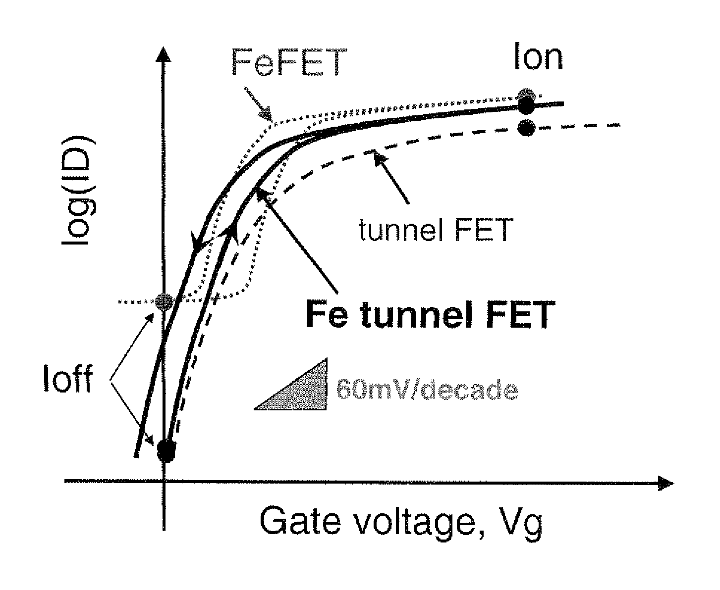
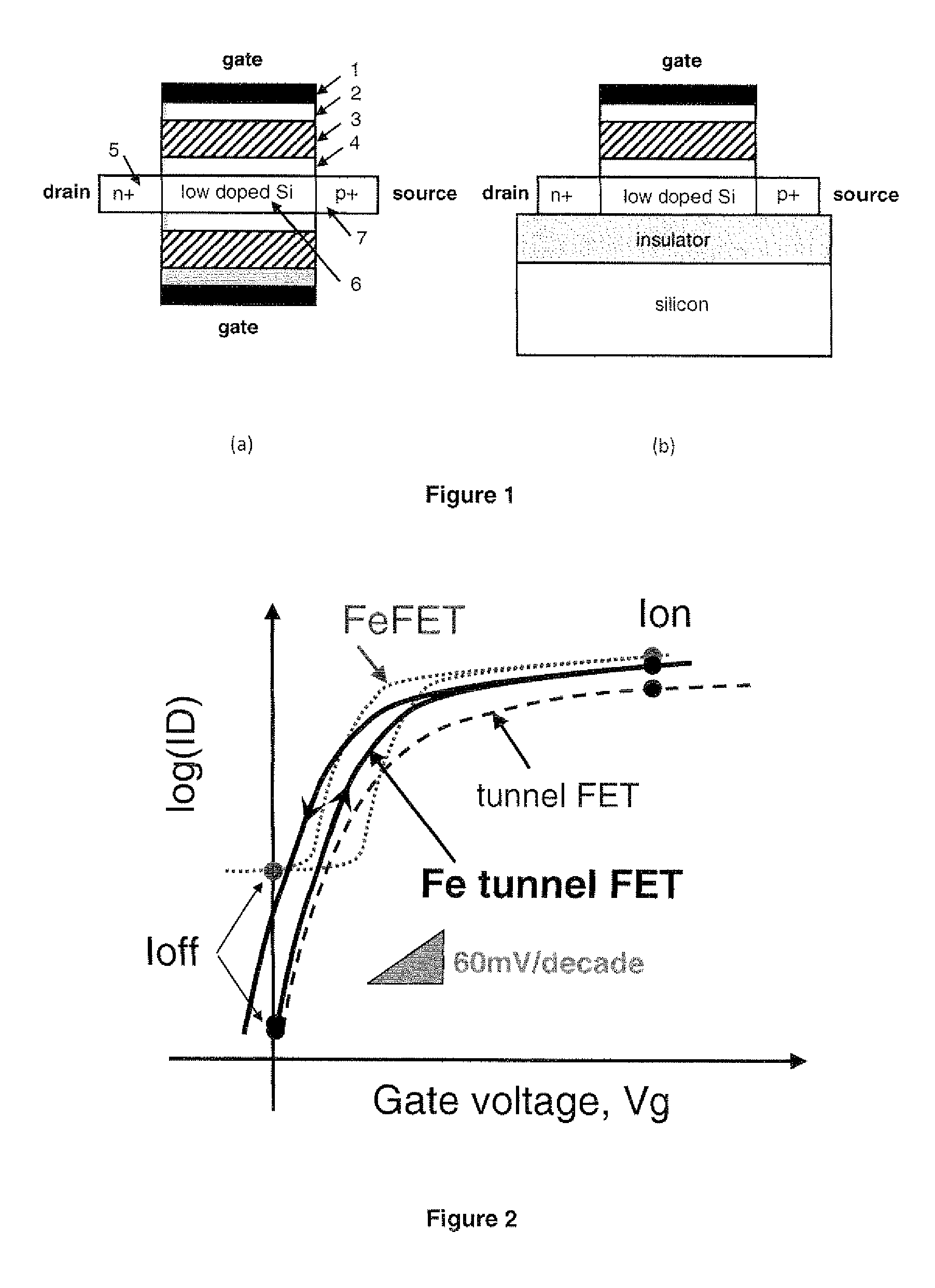
[0018]Ferroelectric n-type tunnel FET embodiments according to the present invention are illustrated in FIGS. 1 (a) and (b). They comprise a tunnel FET based on a gated pin junction and ferroelectric gate stack that controls the tunneling process. The structure could correspond to a double-gate Silicon-On-Insulator or a Gate-All-Around Nanowire FET, depicted by the cross-section of FIG. 1a. The layers involved are at least: a metal or polysilicon gate 1, a dielectric capping layer 2, a ferroelectric material 3, a thin interfacial dielectric (could be silicon dioxide) 4, a highly n-type doped silicon 5, a low doped (or intrinsic) silicon 6 and a highly p-type doped silicon 7.

[0019]Layers 2 (dielectric capping) and 4 (thin interfacial dielectric) are not mandatory for the device operation and may be absent. Layers 5, 6 and 7 may be any other equivalent type of semiconductor and the materials that may be used are not limited to the examples given above.

[0020]FIG. 1b shows a similar imp...


PUM


Abstract

A Ferroelectric tunnel FET switch as ultra-steep (abrupt) switch with subthreshold swing better than the MOSFET limit of 60 mV / decade at room temperature combining two key principles: ferroelectric gate stack and band-to-band tunneling in gated p-i-n junction, wherein the ferroelectric material included in the gate stack creates, due to dipole polarization with increasing gate voltage, a positive feedback in the capacitive coupling that controls the band-to-band (BTB) tunneling at the source junction of a silicon p-i-n reversed bias structure, wherein the combined effect of BTB tunneling and ferroelectric negative capacitance offers more abrupt off-on and on-off transitions in the present proposed Ferroelectric tunnel FET than for any reported tunnel FET or any reported ferroelectric FET.

Description

[0001]This application claims the benefit to U.S. Provisional Application No. 61 / 119,734 filed Dec. 4, 2008, the entire contents of which is hereby incorporated by reference.TECHNICAL FIELD[0002]The present invention concerns the field of tunneling FET (field effect transistors) switches and memory devices. More specifically, the present invention concerns an improved device that is able to offer more abrupt off-on and on-off transitions than any reported tunnel FET or any reported ferroelectric FET of the prior art. The proposed device is capable to offer lower voltage operation compared to traditional FETs of tunnel FETs by combining two switching mechanisms (band-to-band tunneling and negative capacitance) in a single device: a tunnel FET with a ferroelectric gate stack. Moreover, the proposed device can serve as a one transistor memory cell with the Ioff current much lower that any existing one transistor ferroelectric FET.BACKGROUND OF THE INVENTION[0003]Today power dissipation...

Claims


Application Information

Patent Timeline
Patent Type & Authority Patents(United States)
IPC IPC(8): H01L21/60
CPCB82Y10/00B82Y30/00G11C11/22H01L29/0665H01L29/78391H01L29/6684H01L29/7391H01L29/0673H01L29/785H01L29/78645
Inventor IONESCU, MIHAI ADRIAN
Owner ECOLE POLYTECHNIQUE FEDERALE DE LAUSANNE (EPFL)
Why Eureka
Try Eureka