
Via-less thin film resistor with a dielectric cap

a dielectric cap and thin film technology, applied in resistor details, resistive material coatings, basic electric elements, etc., can solve the problems of damage affecting the sheet resistance and temperature coefficient of resistance, and achieve good stability and temperature characteristics, precise resistance values, and heat dissipation

Active Publication Date: 2013-03-19
STMICROELECTRONICS SRL
View PDF42 Cites 15 Cited by
  • Summary
  • Abstract
  • Description
  • Claims
  • Application Information

AI Technical Summary

Benefits of technology

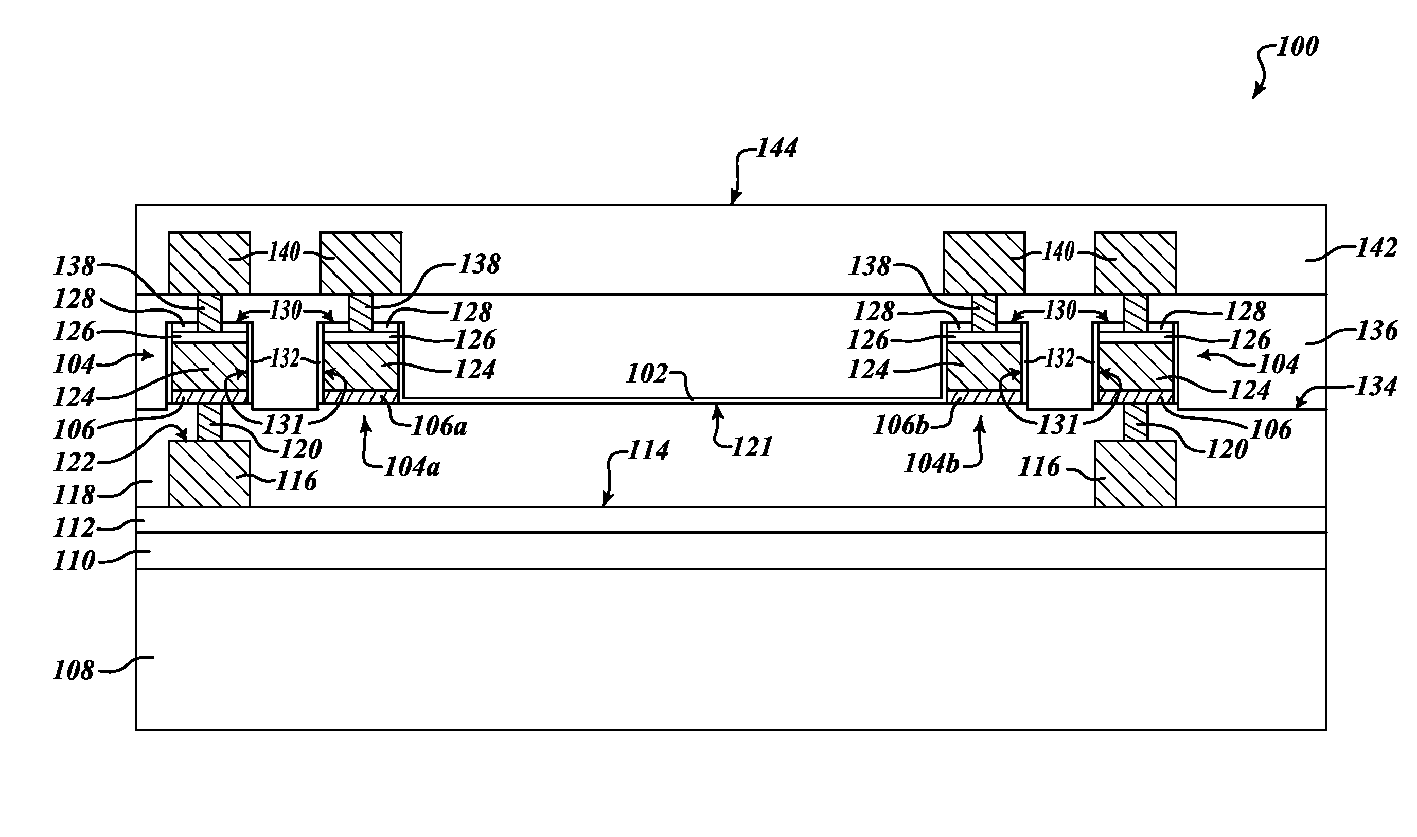
This patent describes a method of protecting sensitive thin film resistors during processing steps. By using a dielectric cap, the resistors are protected from damage caused by plasma etches and are able to achieve precise resistance values in a small area. Additionally, interconnect structures can be connected without using processing steps of forming resistor head contact structures and vias, which saves time and resources. Additionally, the patent also describes a protective coating that prevents damage to the interconnect structures during etch removal, allowing for minimum spacing between interconnect structures. Overall, this patent provides a more efficient and cost-effective method for manufacturing thin film resistors in semiconductor devices.

Problems solved by technology

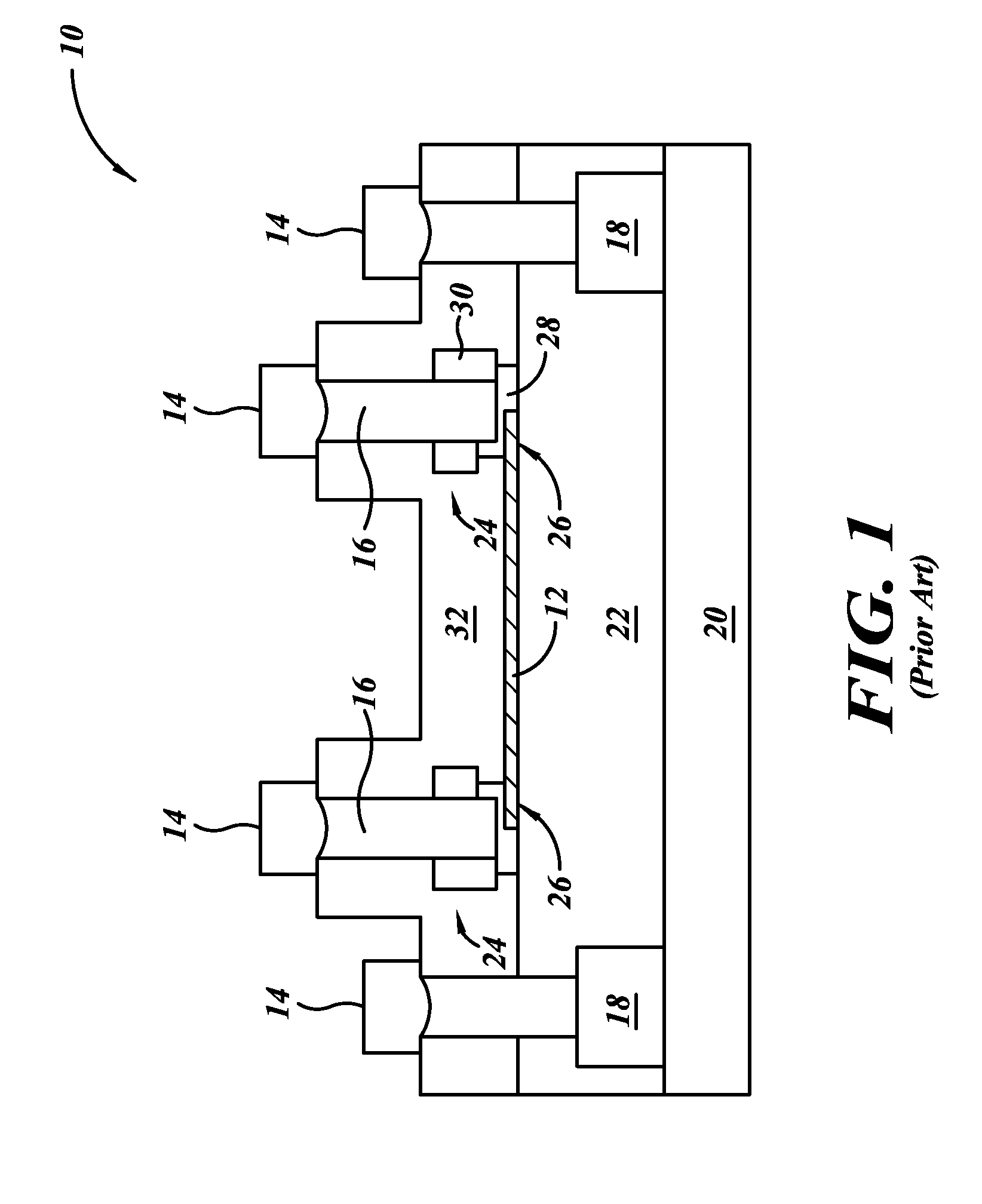
The thin film resistor layer is very sensitive to damage from plasma etches, and if not protected such damage can impact the sheet resistance and temperature coefficient of resistance.

Method used


Image

  • Via-less thin film resistor with a dielectric cap
  • Via-less thin film resistor with a dielectric cap
  • Via-less thin film resistor with a dielectric cap

Examples


Embodiment Construction

[0034]In the following description, certain specific details are set forth in order to provide a thorough understanding of various embodiments of the disclosure. However, one skilled in the art will understand that the disclosure may be practiced without these specific details. In some instances, well-known structures associated with the manufacturing of semiconductor wafers have not been described in detail to avoid obscuring the descriptions of the embodiments of the present disclosure.

[0035]Unless the context requires otherwise, throughout the specification and claims that follow, the word “comprise” and variations thereof, such as “comprises” and “comprising,” are to be construed in an open, inclusive sense, that is, as “including, but not limited to.”

[0036]Reference throughout this specification to “one embodiment” or “an embodiment” means that a particular feature, structure, or characteristic described in connection with the embodiment is included in at least one embodiment. ...


PUM

PropertyMeasurementUnit
thicknessaaaaaaaaaa
sheet resistanceaaaaaaaaaa

Abstract

The present disclosure is directed to a thin film resistor structure that includes a resistive element electrically connecting first conductor layers of adjacent interconnect structures. The resistive element is covered by a dielectric cap layer that acts as a stabilizer and heat sink for the resistive element. Each interconnect includes a second conductor layer over the first conductive layer. The thin film resistor includes a chromium silicon resistive element covered by a silicon nitride cap layer.

Description

BACKGROUND[0001]1. Technical Field[0002]The present disclosure is directed to thin film resistors, and more particularly, to a thin film resistor having a dielectric cap, where the thin film resistor electrically connects conductive layers of adjacent interconnects.[0003]2. Description of the Related Art[0004]Precision resistors provide stable resistances for integrated circuits used in various precision electronic devices, such as pacemakers, printers, and testing or measuring instruments. Each electronic device utilizes specific resistance values and operates in different conditions. Manufacturers tailor precise resistance values for each electronic device by controlling the size of the resistor and by using materials having low temperature and voltage coefficients. However, the performance of these precision resistors is often impacted by variations in operating conditions, like temperature and voltage. Manufacturers strive to achieve tight tolerances with respect to resistance a...

Claims


Application Information

Patent Timeline
Patent Type & Authority Patents(United States)
IPC IPC(8): H01C1/012H10N97/00
CPCH01L21/76834H01L21/76852H01L23/5228H01L28/20H01C1/148H01C7/006Y10T29/49099H01L2221/1078H01L28/24H01L2924/0002H01L2924/00
Inventor LIM, TING FANGNIU, CHENGYULE NEEL, OLIVIERLEUNG, CALVIN
Owner STMICROELECTRONICS SRL
Learn More