Resist coating and developing apparatus and method

a technology of resist coating and developing apparatus, which is applied in the field of resist coating and developing, can solve the problems of affecting the development of resist film, affecting the patterning of resist film, and affecting the quality of resist film, so as to reduce the roughness of resist pattern lines and avoid contamination of process atmospher

Active Publication Date: 2013-04-02
TOKYO ELECTRON LTD
View PDF19 Cites 2 Cited by
  • Summary
  • Abstract
  • Description
  • Claims
  • Application Information

AI Technical Summary

Benefits of technology

[0008]The present invention provides a resist coating / developing apparatus and a resist coating / developing method, which can effectively reduce the line width roughness of a resist pattern while preventing a solvent gas from diffusing outside.
[0011]The embodiments of the resist coating / developing apparatus and method according to the present invention can effectively reduce the line width roughness of a resist pattern while avoiding contamination of the process atmosphere.

Problems solved by technology

In the formation of the channel of a field-effect transistor (FET), having such a width, a large line width roughness (LWR) of resist pattern will lead to variation in the threshold voltage of the FET, causing problems such as worsening of properties or abnormal operation of the resulting integrated circuit.
In the case where the resist film is formed of a chemically-amplified resist, an acidic component in the resist film can be neutralized by an alkaline component contained in the solvent, which may inhibit development of the resist film and can even make patterning of the resist film impossible.
If a gas of such a solvent leaks from a resist coating / developing apparatus into the surrounding space, the diffused gas will give an unpleasant feeling to an operator of the apparatus.

Method used


Image

  • Resist coating and developing apparatus and method
  • Resist coating and developing apparatus and method
  • Resist coating and developing apparatus and method

Examples


Embodiment Construction

[0023]Non-limitative exemplary embodiments of the present invention will now be described with reference to the drawings. In the drawings, the same reference numerals are used for the same or equivalent members or components, and a duplicate description thereof will be omitted.

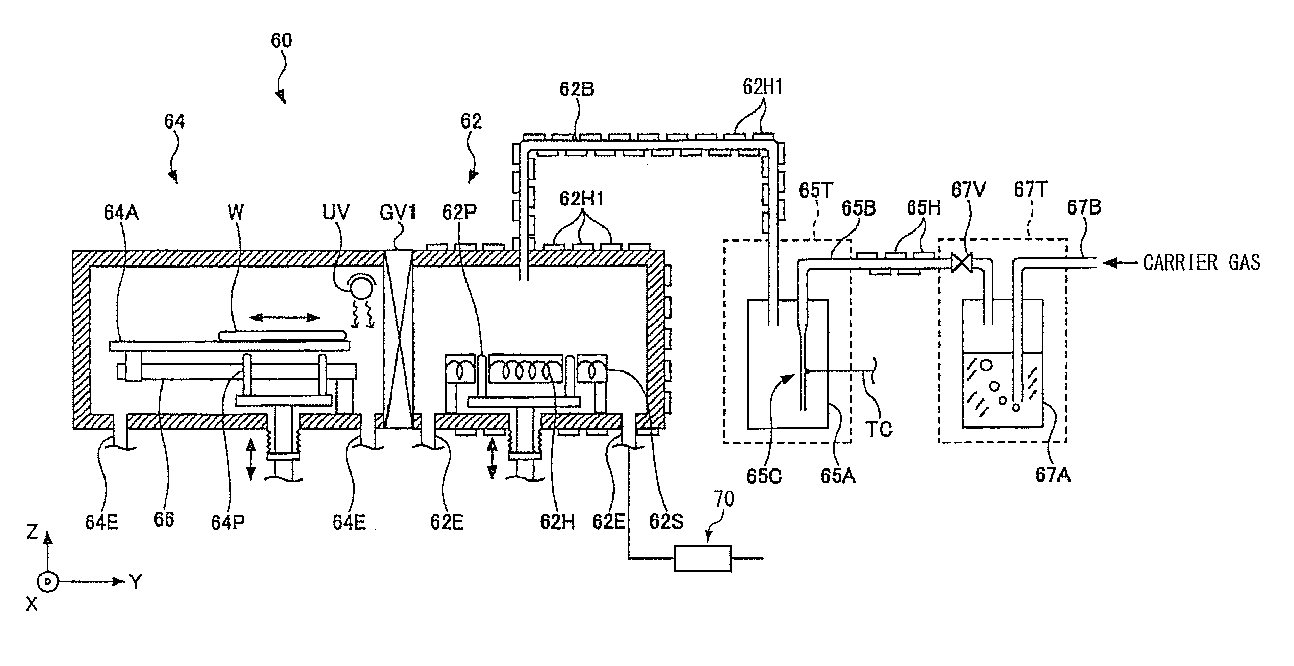
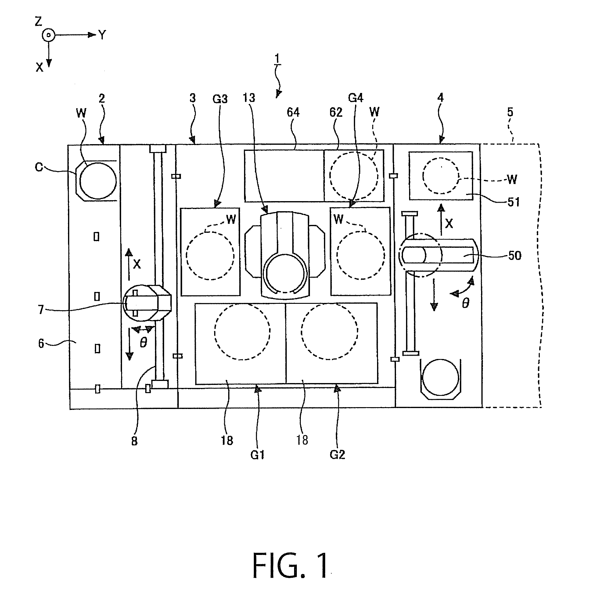
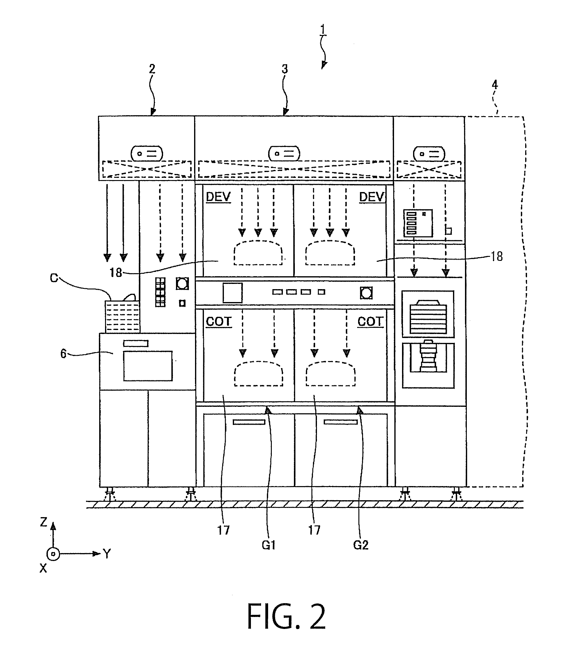
[0024]FIG. 1 is a schematic plan view showing the construction of a resist coating / developing apparatus 1 according to an embodiment of the present invention; FIG. 2 is a schematic front view of the resist coating / developing apparatus 1; and FIG. 3 is a schematic back view of the resist coating / developing apparatus 1. As shown in FIG. 1, the resist coating / developing apparatus 1 includes a cassette station 2, a processing station 3 and an interface section 4.

[0025]The cassette station 2 includes a stage section 6 on which a cassette C, e.g. housing 25 wafers, is placed, and a wafer transporter 7 for taking a wafer W out of the cassette C placed on the stage section 6, and transferring the wafer W between the c...


PUM


Abstract

A resist coating / developing apparatus includes: a resist film-forming unit configured to apply a resist onto a substrate to form thereon a resist film; a resist developing unit configured to develop the resist film after exposure to pattern the resist film; a solvent gas generator configured to generate a solvent gas containing a vapor of a solvent having a property of dissolving the resist film; a solvent gas conditioner connected to the solvent gas generator and configured to condition the solvent gas generated in the solvent gas generator; a processing chamber configured to house the substrate having thereon the resist film which has been developed and patterned in the resist developing unit, and connected to the solvent gas conditioner so that the solvent gas, which has been conditioned in the solvent gas conditioning section, is supplied to the substrate housed in the processing chamber; and an exhaust system connected to the processing chamber to evacuate the processing chamber to a reduced pressure.

Description

BACKGROUND OF THE INVENTION[0001]1. Field of the Invention[0002]The present invention relates to a resist coating and developing (hereinafter abbreviated as “coating / developing”) apparatus and method for coating a substrate with a resist film, and developing the resist film after exposure to form a resist pattern, and more particularly to a resist coating / developing apparatus and method which, by flattening the resist pattern, can reduce the line width roughness of the resist pattern.[0003]2. Description of Related Art[0004]In order to manufacture semiconductor integrated circuits with higher levels of integration, there is a demand for the production of finer circuit patterns. For example, the critical dimension of (CD) of an etching mask is reaching 32 nm or even 22 nm, which values are lower than the resolution limits of existing exposure apparatuses. In the formation of the channel of a field-effect transistor (FET), having such a width, a large line width roughness (LWR) of res...

Claims


Application Information

Patent Timeline
Patent Type & Authority Patents(United States)
IPC IPC(8): G03B27/32G03B27/52B05C11/00
CPCG03F7/40H01L21/67017H01L21/67109H01L21/67115H01L21/6715H01L21/6719H01L21/67748G03F7/2041G03F7/70625G03F7/70916H01L21/0274
Inventor INATOMI, YUICHIRO
Owner TOKYO ELECTRON LTD
Why Eureka
Try Eureka