Optical device structure using miscut GaN substrates for laser applications
Active Publication Date: 2013-04-16
KYOCERA SLD LASER INC
View PDF100 Cites 190 Cited by
Summary
Abstract
Description
Claims
Application Information
AI Technical Summary
This helps you quickly interpret patents by identifying the three key elements:
Problems solved by technology
Method used
Benefits of technology
[0017]Benefits are achieved over pre-existing techniques using the present invention. In particular, the present invention enables a cost-effective optical device for laser applications. In a specific embodiment, the present optical device can be manufactured in a relatively simple and cost effective manner. Depending upon the embodiment, the present apparatus and method can be manufactured using conve
Problems solved by technology
First, the conventional light bulb dissipates much thermal energy. More than 90% of the energy used for the conventional light bulb dissipates as thermal energy.
Secondly, reliability is an issue since the conventional light bulb routinely fails often due to thermal expansion and contraction of the filament element.
Thirdly, light bulbs emit light over a broad spectrum, much of which does not result in bright illumination or due to the spectral sensitivity of the human eye.
Lastly, light bulbs emit in all directions and are not ideal for applications requiring strong directionality or focus such as projection displays, optical data storage, or specialized directed lighting.
The Ar-ion laser had the benefit of producing highly directional and focusable light with a narrow spectral output, but the wall plug efficiency was <0.1%, and the size, weight, and cost of the lasers were undesirable as well.
As laser technology evolved, more efficient lamp pumped solid state laser designs were developed for the red and infrared wavelengths, but these technologies remained a challenge for blue and green and blue lasers.
The resulting green and b
Method used
Image
Click on the blue label to locate the original text in one second.
Reading with bidirectional positioning of images and text.
Examples
Embodiment Construction
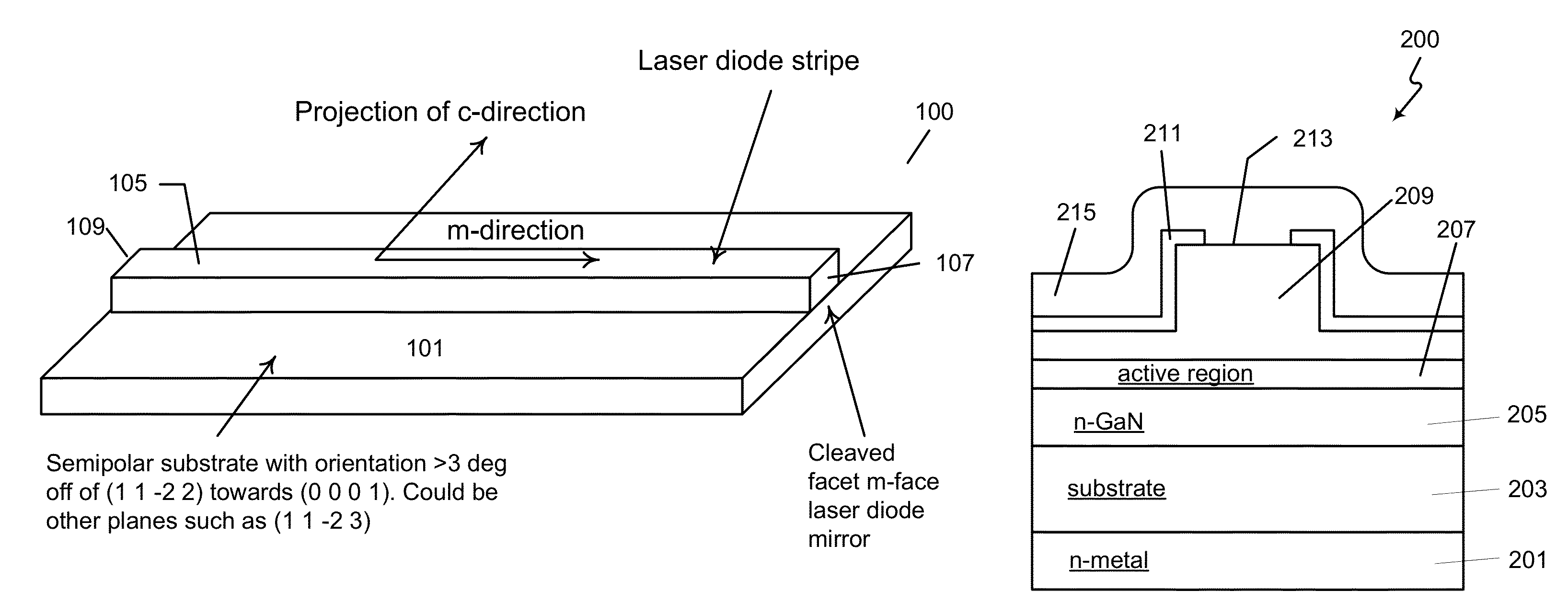
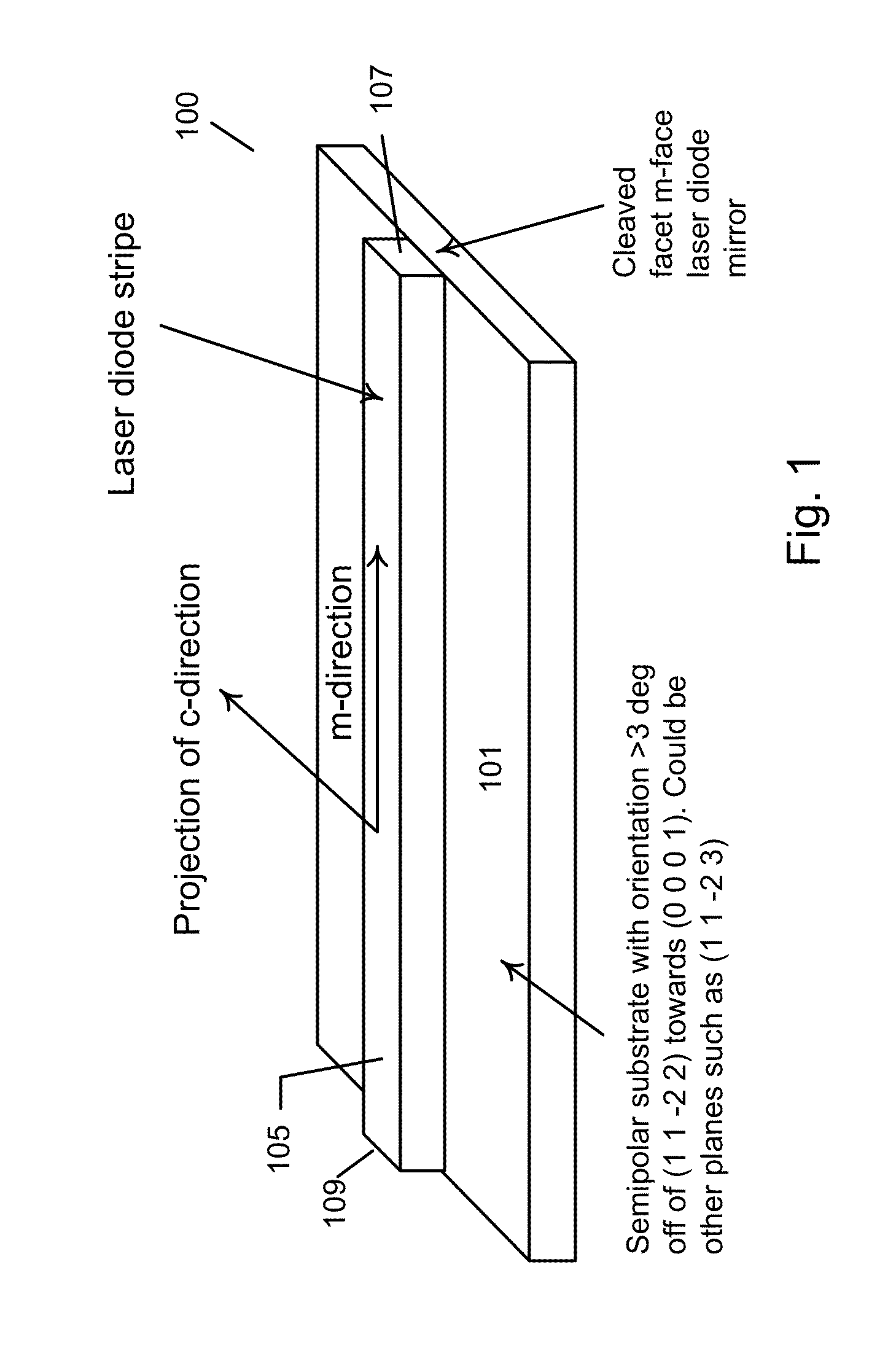
[0025]In a specific embodiment, the (11-22) GaN crystallographic plane is desirable in the field of GaN optoelectronic devices due to its high indium uptake in InGaN films that enable efficient light emission into the green wavelength region. Furthermore, it has been discovered that the m-face of the (11-22) substrate can be cleaved to form laser facet quality surfaces, which is believed to be one of the key characteristics for manufacturing low cost laser diodes. In order to use such cleave plane, the laser stripes are preferably oriented in the m-direction on the substrate surface such that the stripe is normal to the mirror. By the rules of electromagnetics, the polarization of the light generated in the semiconductor is generally orthogonal to the propagation direction, which in the case of a laser is in the stripe direction. The polarization of the light is governed by the valence band structure within the semiconductor crystal. It has also discovered that when increasing the i...
PUM
Abstract
An optical device capable of emitting light having a wavelength ranging from about 490 to about 580 nanometers has a gallium nitride substrate with a semipolar crystalline surface region characterized by an orientation of greater than 3 degrees from (11-22) towards (0001) but less than about 50 degrees. A laser stripe formed on the substrate has a cavity orientation substantially parallel to the m-direction.
Description
CROSS-REFERENCES TO RELATED APPLICATIONS[0001]This application claims priority to U.S. Provisional Application No. 61 / 164,409 filed Mar. 28, 2009, commonly assigned, and incorporated by reference in its entirety for all purpose herein.BACKGROUND OF THE INVENTION[0002]The present invention is directed to optical devices and related methods. More particularly, the present invention provides a method and device for emitting electromagnetic radiation using semipolar gallium containing substrates such as GaN, MN, InN, InGaN, AlGaN, and AlInGaN, and others. Merely by way of example, the invention can be applied to optical devices, lasers, light emitting diodes, solar cells, photoelectrochemical water splitting and hydrogen generation, photodetectors, integrated circuits, and transistors, among other devices.[0003]In the late 1800's, Thomas Edison invented the light bulb. The conventional light bulb, commonly called the “Edison bulb,” has been used for over one hundred years for a variety ...
Claims
Application Information
Patent Timeline
Application Date:The date an application was filed.
Publication Date:The date a patent or application was officially published.
First Publication Date:The earliest publication date of a patent with the same application number.
Issue Date:Publication date of the patent grant document.
PCT Entry Date:The Entry date of PCT National Phase.
Estimated Expiry Date:The statutory expiry date of a patent right according to the Patent Law, and it is the longest term of protection that the patent right can achieve without the termination of the patent right due to other reasons(Term extension factor has been taken into account ).
Invalid Date:Actual expiry date is based on effective date or publication date of legal transaction data of invalid patent.