Stress memorization with reduced fringing capacitance based on silicon nitride in MOS semiconductor devices

a semiconductor device and silicon nitride technology, applied in the field of integrated circuits, can solve the problems of reduced controllability of the channel, increased leakage current, shrinkage of the transistor dimension, etc., and achieve the effect of avoiding the negative impact of any spacer element, enhancing the performance of the transistor, and increasing the permittivity

Inactive Publication Date: 2013-04-23
GLOBALFOUNDRIES INC
View PDF15 Cites 6 Cited by
  • Summary
  • Abstract
  • Description
  • Claims
  • Application Information

AI Technical Summary

Benefits of technology

[0013]Generally, the present disclosure provides techniques and semiconductor devices wherein transistor performance may be enhanced on the basis of tensile strain created by using stress memorization techniques, while substantially avoiding a negative impact of any spacer elements formed from the silicon and nitrogen-containing spacer layer, for instance in terms of increased permittivity and the like. To this end, the nitrogen contents of the spacer layer may be reduced after the process for re-crystallizing portions of the active regions of transistors in a highly strained state, thereby enabling the continuation of the further processing by forming spacer elements from the modified spacer layer, which may thus have a significantly reduced dielectric constant. The modification of the nitrogen-containing spacer layer may, in some illustrative aspects disclosed herein, be accomplished by incorporating an oxygen species, for instance by ion implantation, and by treating a spacer layer so as to remove at least a portion of the nitrogen species, thereby obtaining a significantly reduced k value of the resulting modified spacer layer. Consequently, stress memorization techniques may be applied on the basis of the highly efficient nitrogen-containing spacer base material, while, at the same time, the finally obtained spacer elements may exhibit a reduced permittivity compared to conventional strategies. Therefore, the principles disclosed herein may be efficiently applied to sophisticated semiconductor devices including planar transistor configurations with a gate length of, for instance, 40 nm and less, wherein the stress memorization technique is “self-scaling,” as long as corresponding spacer elements may be required for adjusting the profile of drain and source regions and / or for determining a lateral offset of metal silicide regions and the like. Furthermore, since typically sidewall spacer technologies may be applied in many other concepts for implementing transistors, such as three-dimensional configurations in the form of double channel, triple channel or finFET transistors, the stress memorization techniques disclosed herein may also be efficiently applied in any such three-dimensional structures without negatively contributing to an increased parasitic capacitance.

Problems solved by technology

The continuing shrinkage of the transistor dimensions, however, involves a plurality of issues associated therewith, such as reduced controllability of the channel, also referred to as short channel effects, and the like, that have to be addressed so as to not unduly offset the advantages obtained by steadily decreasing the channel length of MOS transistors.
For instance, the thickness of the gate insulation layer, typically an oxide-based dielectric, has to be reduced with reducing the gate length, wherein a reduced thickness may result in increased leakage currents, thereby posing limitations for oxide-based gate insulation layers at approximately 1-2 nm.
Thus, for different transistor types, differently stressed overlayers have to be provided, which may result in a plurality of additional process steps, wherein, in particular, any additional lithography steps may significantly contribute to the overall production costs.
Moreover, the amount of stress-inducing material and in particular the intrinsic stress thereof may not be arbitrarily increased without requiring significant design alterations.
Furthermore, upon further scaling the transistor dimensions, the lateral offset between adjacent gate electrode structures of transistors is also reduced, thereby significantly restricting the possibility of depositing highly stressed dielectric materials above the closely spaced transistor elements.
The well-established silicon / germanium material may be provided in P-channel transistors in order to obtain a high compressive strain, while, on the other hand, tensile strain semiconductor alloys, such as silicon / carbon, may not provide comparable high strain levels due to manufacturing-related issues in providing efficient silicon / carbon material compositions.
Although stress memorization techniques, possibly in combination with efficient silicon / germanium-based strain-inducing mechanisms for P-channel transistors, represent a promising approach for enhancing performance upon further scaling the overall dimensions of transistor elements, other negative influences may have an increasing effect on the overall performance of the transistors.
Similarly, due to the reduced dimensions, the parasitic capacitance of the interconnect elements for providing signals and supply voltages to the highly scaled transistors may increasingly reduce overall performance of the transistors.
For example, the fringing capacitance of the gate electrode, i.e., the parasitic capacitance generated between any contact elements and the gate electrode of the transistors, may increasingly contribute to an inferior high frequency behavior of the transistors, wherein the overall dielectric constant of the dielectric material enclosing the gate electrode structure may be one of the dominant contributors to an increased parasitic capacitance.
Although using the strain-inducing silicon nitride layer as a spacer material provides a very efficient overall process flow, the presence of the silicon nitride material in the form of a sidewall spacer element at the gate electrode structures may cause an increased parasitic capacitance due to the moderately high-k value of silicon nitride material.
On the other hand, the removal of the silicon nitride layer after generating the desired tensile strain component may result in undue process complexity.

Method used


Image

  • Stress memorization with reduced fringing capacitance based on silicon nitride in MOS semiconductor devices
  • Stress memorization with reduced fringing capacitance based on silicon nitride in MOS semiconductor devices
  • Stress memorization with reduced fringing capacitance based on silicon nitride in MOS semiconductor devices

Examples


Embodiment Construction

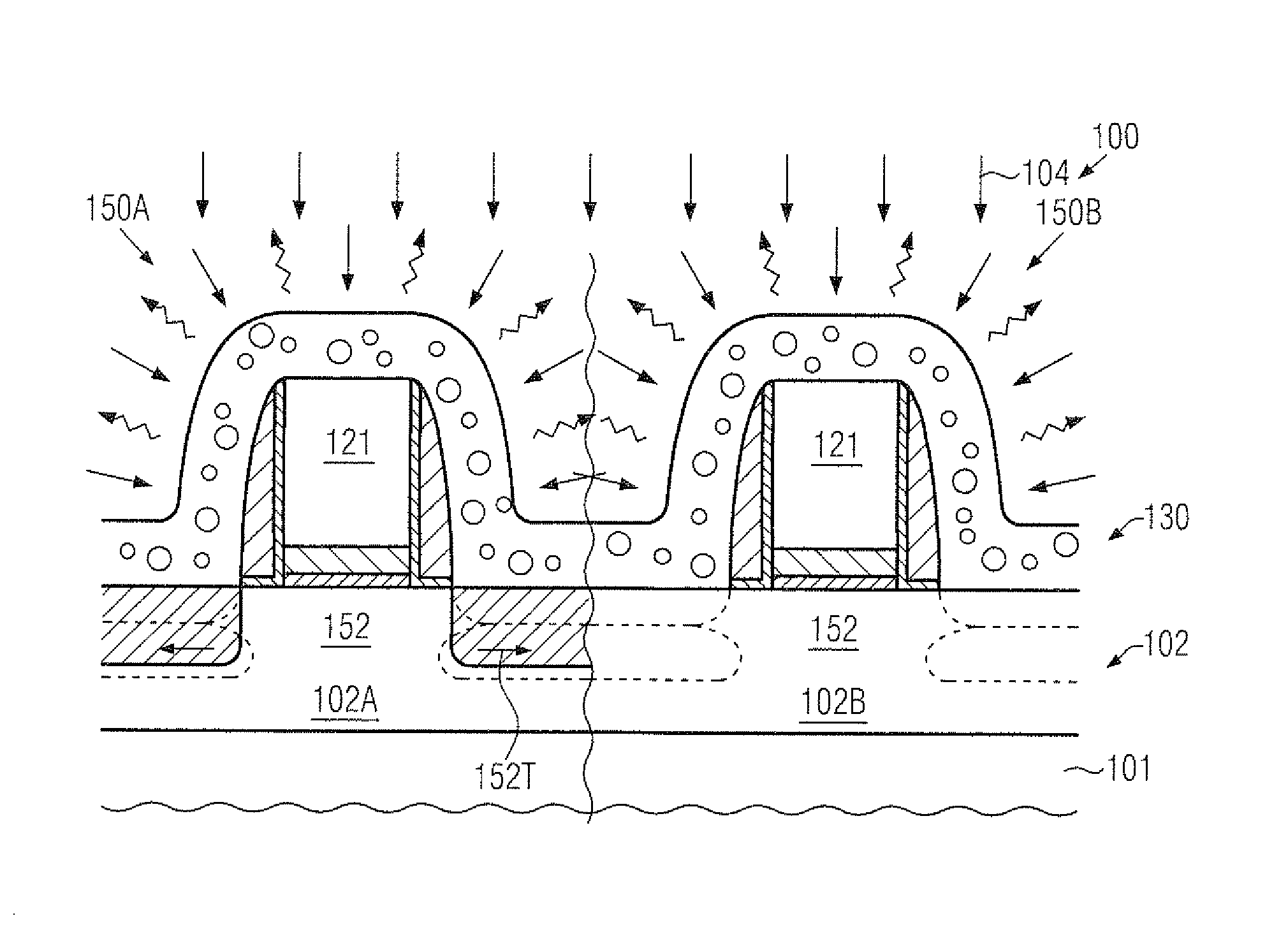
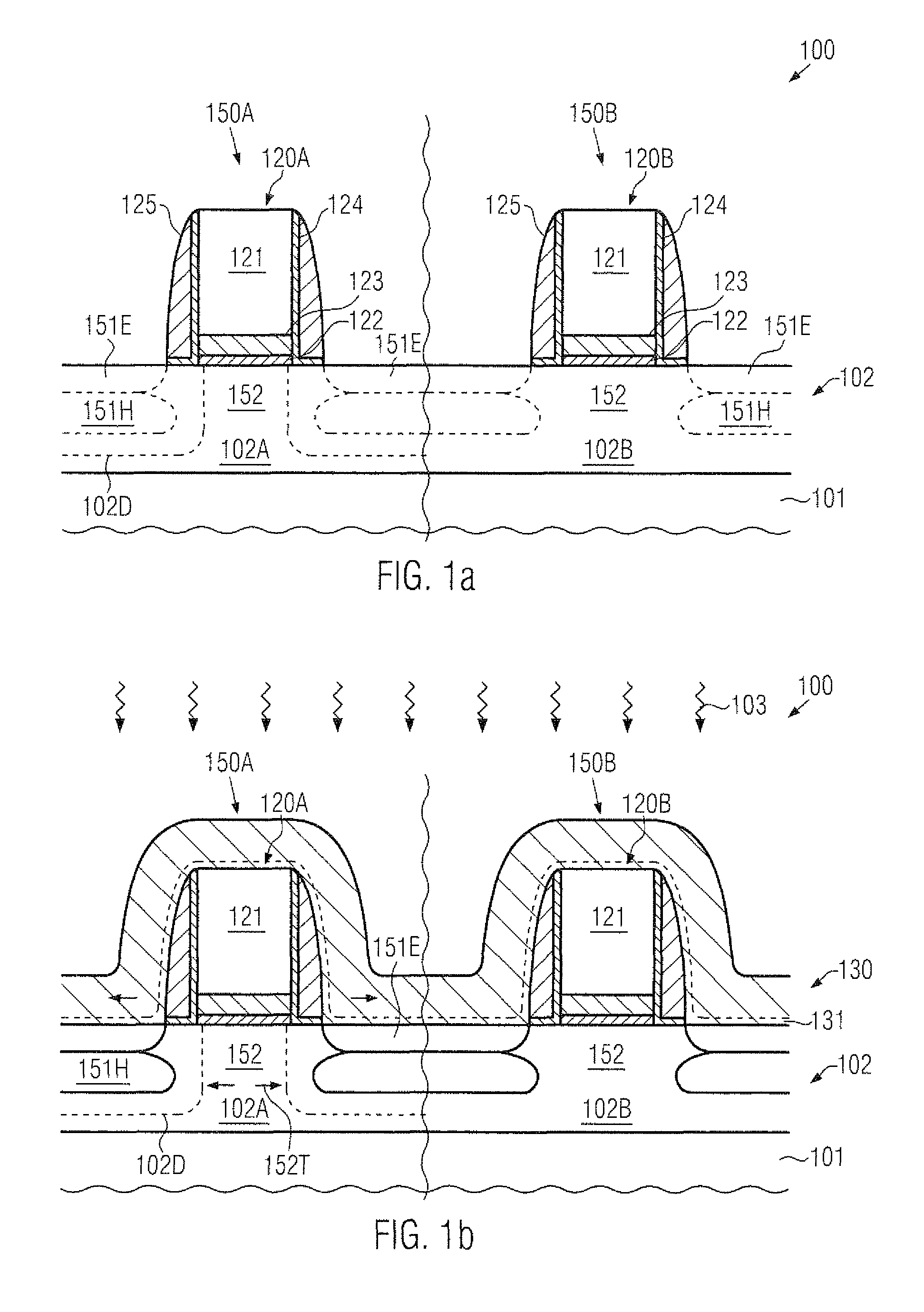
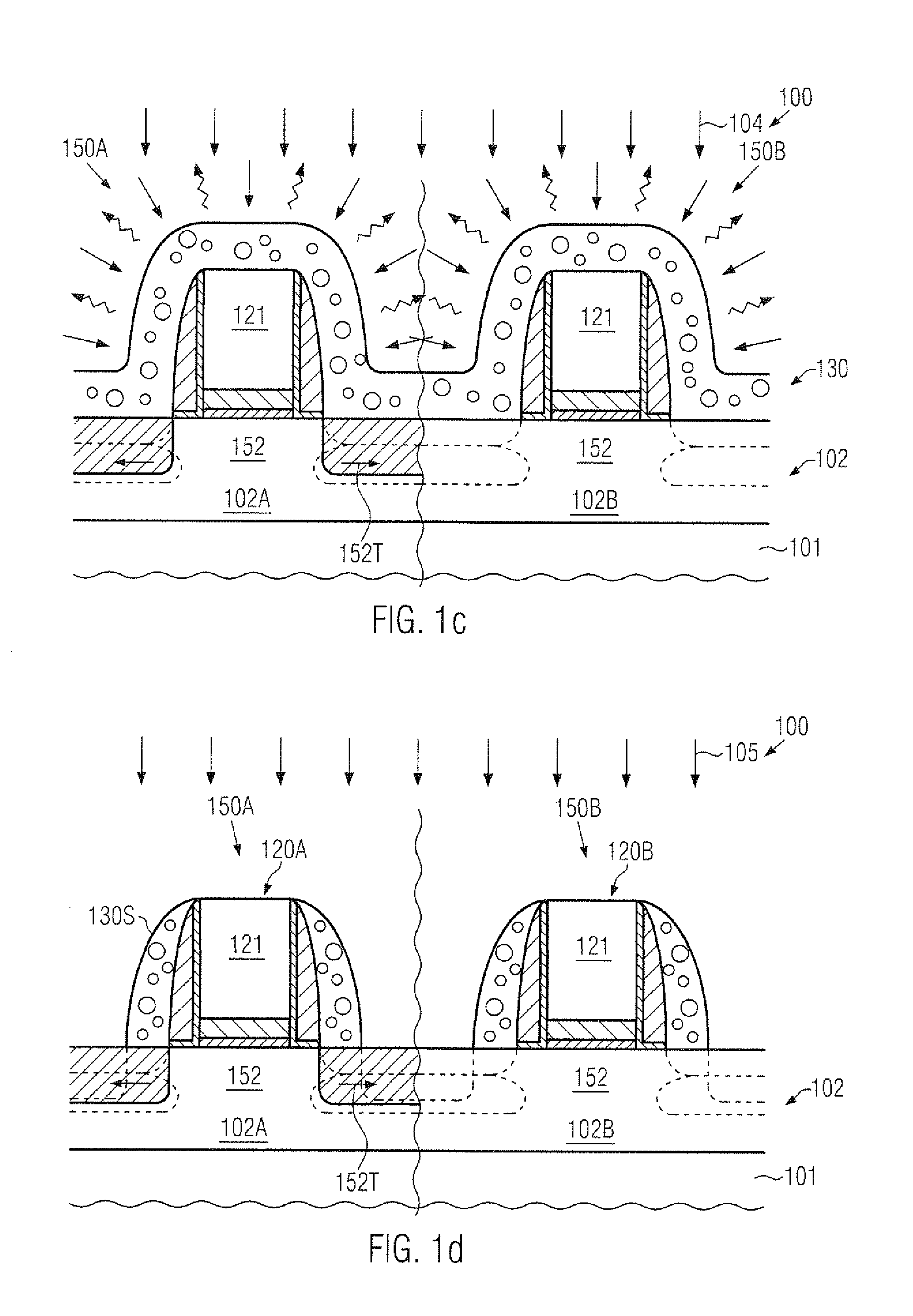
[0021]Various illustrative embodiments of the invention are described below. In the interest of clarity, not all features of an actual implementation are described in this specification. It will of course be appreciated that in the development of any such actual embodiment, numerous implementation-specific decisions must be made to achieve the developers' specific goals, such as compliance with system-related and business-related constraints, which will vary from one implementation to another. Moreover, it will be appreciated that such a development effort might be complex and time-consuming, but would nevertheless be a routine undertaking for those of ordinary skill in the art having the benefit of this disclosure.

[0022]The present subject matter will now be described with reference to the attached figures. Various structures, systems and devices are schematically depicted in the drawings for purposes of explanation only and so as to not obscure the present disclosure with details ...


PUM

PropertyMeasurementUnit
gate lengthaaaaaaaaaa
thicknessaaaaaaaaaa
dielectric constantaaaaaaaaaa

Abstract

In sophisticated semiconductor devices, stress memorization techniques may be applied on the basis of a silicon nitride material, which may be subsequently modified into a low-k dielectric material in order to obtain low-k spacer elements, thereby enhancing performance of sophisticated semiconductor devices. The modification of the initial silicon nitride-based spacer material may be accomplished on the basis of an oxygen implantation process.

Description

BACKGROUND OF THE INVENTION[0001]1. Field of the Invention[0002]Generally, the present disclosure relates to integrated circuits, and, more particularly, to transistors having strained channel regions by using stress memorization techniques so as to enhance charge carrier mobility in the channel region of a MOS transistor.[0003]2. Description of the Related Art[0004]Generally, a plurality of process technologies are currently practiced to fabricate integrated circuits, wherein, for complex circuitry, such as microprocessors, storage chips and the like, CMOS technology is currently one of the most promising approaches due to the superior characteristics in view of operating speed and / or power consumption and / or cost efficiency. During the fabrication of complex integrated circuits using CMOS technology, millions of transistors, i.e., N-channel transistors and P-channel transistors, are formed on a substrate including a crystalline semiconductor layer. A MOS transistor, irrespective o...

Claims


Application Information

Patent Timeline
Patent Type & Authority Patents(United States)
IPC IPC(8): H01L21/8238
CPCH01L21/265H01L21/26506H01L21/823807H01L21/823814H01L21/823864H01L29/4983H01L29/6653H01L29/6656H01L29/7833H01L29/7847H01L21/268H01L29/6659
Inventor HOENTSCHEL, JANKURZ, ANDREASGRIEBENOW, UWESCHEIPER, THILO
Owner GLOBALFOUNDRIES INC
Why Eureka
Try Eureka