

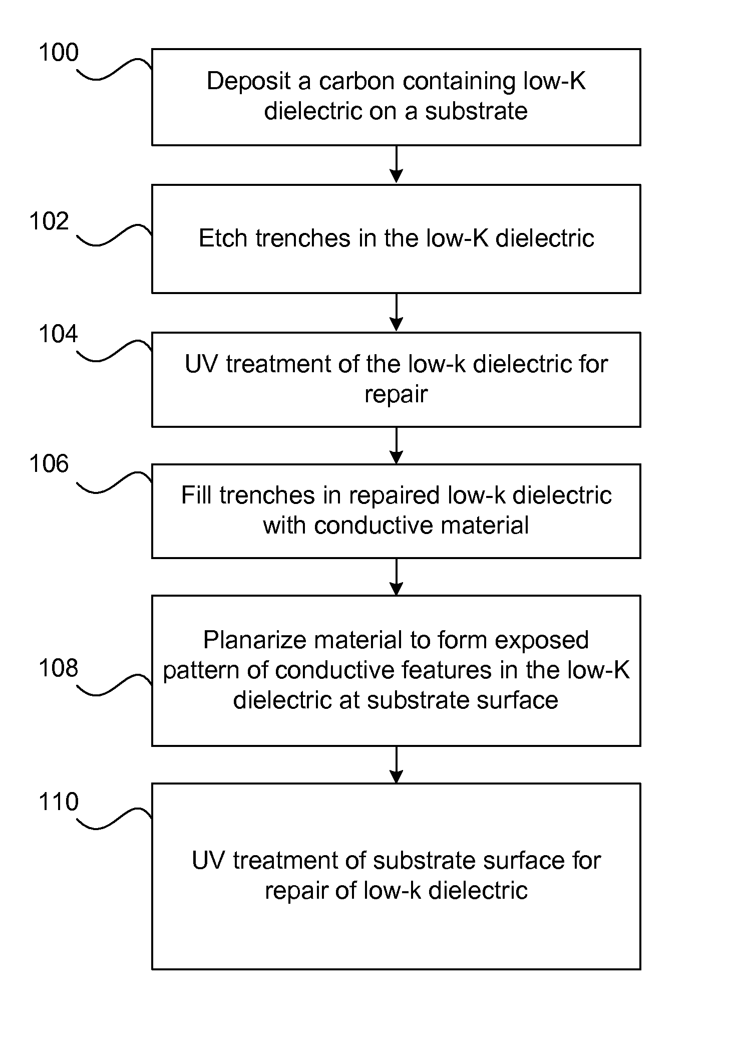
Carbon containing low-k dielectric constant recovery using UV treatment
a technology of uv treatment and dielectric constant, which is applied in the field of low-k dielectric constant layers in semiconductor processing, can solve the problems of inherently weak low-k dielectric materials, affecting the degree of k-recovery, so as to reduce or minimize the shrinkage of dielectrics and enhance the extent of k-recovery
- Summary
- Abstract
- Description
- Claims
- Application Information
AI Technical Summary
Benefits of technology
Problems solved by technology
Method used
Image

Examples
examples
[0093]The following provides examples of specific implementations of the present invention and performance data in order to give a better understanding of the operation and benefits of the invention. The invention is, however, in no way limited to these specific implementations.
[0094]Post-CMP k Recovery Using UV Treatment
[0095]As part of the solution to lower RC delay, materials with significantly lower k (k<2.60) are being used as ILD materials. The typical way to reduce the k is through incorporation of porogen in these materials, which is eventually driven out and the film is cross-linked to increase its hardness (typically using UV).
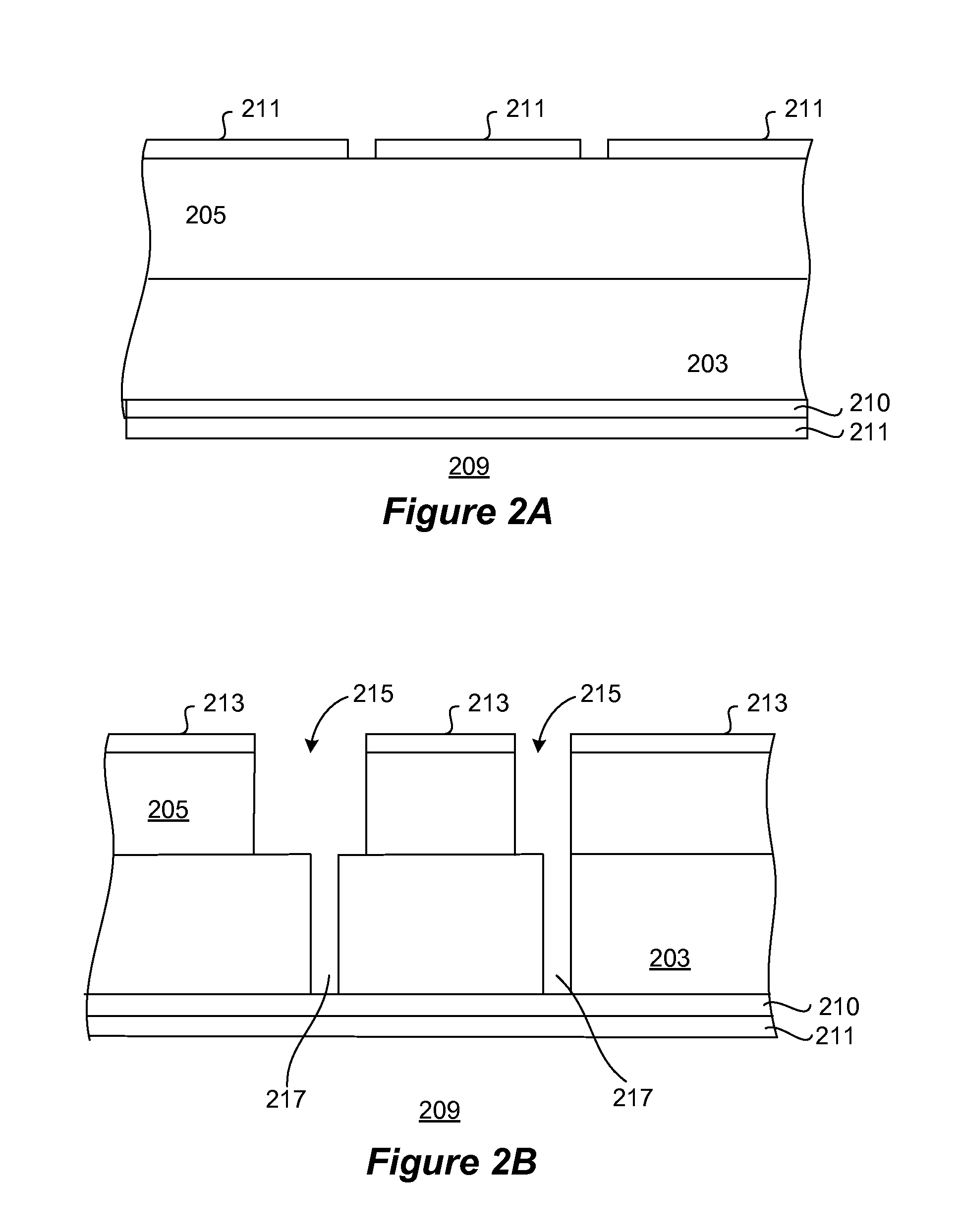
[0096]After electroplating of copper, it is planarized using CMP. These porous ULK materials are susceptible to CMP damage. Some amount of C removal occurs from the surface of these films, with consequent moisture intake resulting in an increase in its dielectric constant.
[0097]The next step in the process is deposition of a dielectric barrier / etch s...
PUM
| Property | Measurement | Unit |
|---|---|---|
| wavelength | aaaaa | aaaaa |
| wavelength range | aaaaa | aaaaa |
| wavelength range | aaaaa | aaaaa |
Abstract
Description
Claims
Application Information