Organic electroluminescent device

a technology of electroluminescent devices and organic materials, which is applied in the direction of discharge tubes/lamp details, luminescent compositions, discharge tubes/lamp details, etc., can solve the problems of inability to change the design (including the thickness of the layer) of the electroluminescent device unlimitedly, poor adhesion of magnesium to the surface of organic materials, and inability to oxidize and stable magnesium. , to achieve the effect of reducing the energy barrier, low voltag

Active Publication Date: 2013-10-15
MITSUBISHI HEAVY IND LTD +1
View PDF44 Cites 2 Cited by
  • Summary
  • Abstract
  • Description
  • Claims
  • Application Information

AI Technical Summary

Benefits of technology

[0022]The present invention is devised in view of the above-described problems of the prior art organic EL devices. The object of the present invention is to lower a driving voltage of the EL device by reducing an energy barrier generated during injection of holes from an anode electrode layer to an organic compound layer in the EL device, and at the same time, by utilizing the much lower resistivity of the hole injection layer, newly introduced into the EL device in accordance with the present invention, on different scales than that of other available organic layers, to control a layer thickness of the hole injection layer without being substantially restrained by its upper limit, thereby largely diminishing a risk of the electrical short circuit between the cathode electrode layer and the anode electrode layer without increasing a driving voltage.
[0023]Further, it is another object of the present invention to enable the hole injection layer which is a mixed layer of a metal oxide and an organic compound to act as a barrier for diminishing any damages due to high energy particles caused during the formation of electrodes using a sputtering method.
[0024]Furthermore, the inventors of the present invention have suggested an organic EL device having a novel structure-which is different from the structure of prior art organic EL devices. This EL device is characterized in that two or more light-emissive units, which correspond to a portion of the layers sandwiched by the cathode electrode layer and the anode electrode layer in the prior art devices, are partitioned with a layer called a “charge-generation layer”, and the charge-generation layer can act as a layer for generating holes and electrons during application of the voltage, thereby resulting in multiple and simultaneous light emission in the EL device as is observed when two or more prior art EL devices are connected in series.
[0025]In the above EL device, it was expected that the charge-generation layer can act as an electron injection layer or a hole injection layer when it is disposed in adjacent to the cathode electrode layer or the anode electrode layer, because the charge-generation layer can act as a hole injection layer to the light-emissive unit adjacent and disposed on a side of the cathode electrode layer thereof, and also the charge-generation layer can act as an electron injection layer to the light-emissive unit adjacent and disposed on a side of the anode electrode layer thereof. Accordingly, the present invention uses this structure of the charge-generation layer in a layer adjacent to the anode electrode layer, thereby enabling low voltage driving and stable driving of the EL devices.
[0028]The present invention is also devised in view of these circumstances, and thus the present invention disposes, adjacent to the anode electrode layer, a hole injection layer having a novel structure capable of diminishing an energy barrier generated during injection of holes from the anode electrode layer, thereby achieving an organic EL device having a low voltage drivability and a driving stability.

Problems solved by technology

However, since magnesium is liable to be oxidized and instable and also has poor adhesion to the surface of the organic material, Tang et al. have suggested to use magnesium alloyed with silver (Ag: work function of 4.6 eV), since silver is relatively stable, and thus has a high work function and good adhesion to the surface of the organic material.
Furthermore, in the Kodak patents described above, it is disclosed that the alkaline metals having the lowest work function, should be removed from the candidate examples of the cathode metal, even though they can exhibit excellent function in principle, because they have an excessively high reactivity for achieving the stable driving of the EL devices.
On the other hand, generally, many of the Lewis acid compounds are chemically instable and therefore they suffer from poor storage stability.
The hole injection layer using an organic compound having a small ionization potential, suggested by Tang et al. and Shirota et al., can improve a compatibility with the anode electrode layer, however, due to the upper limit of the applicable layer thickness, a layer design (including layer thickness) of the EL devices cannot be unlimitedly changed.
Similarly, the lamination of a metal oxide having a large work function on the anode electrode layer, suggested by Toyota CRDL Inc., suffers from limitation in the applicable layer thickness due to low light transmittance of the metal oxide, and the limitation that substantially all of the exemplified compounds can only be deposited with a sputtering method.

Method used


Image

  • Organic electroluminescent device
  • Organic electroluminescent device
  • Organic electroluminescent device

Examples


example 1

[0095]In this example, the organic EL device having the lamination structure of FIG. 5 is fabricated.

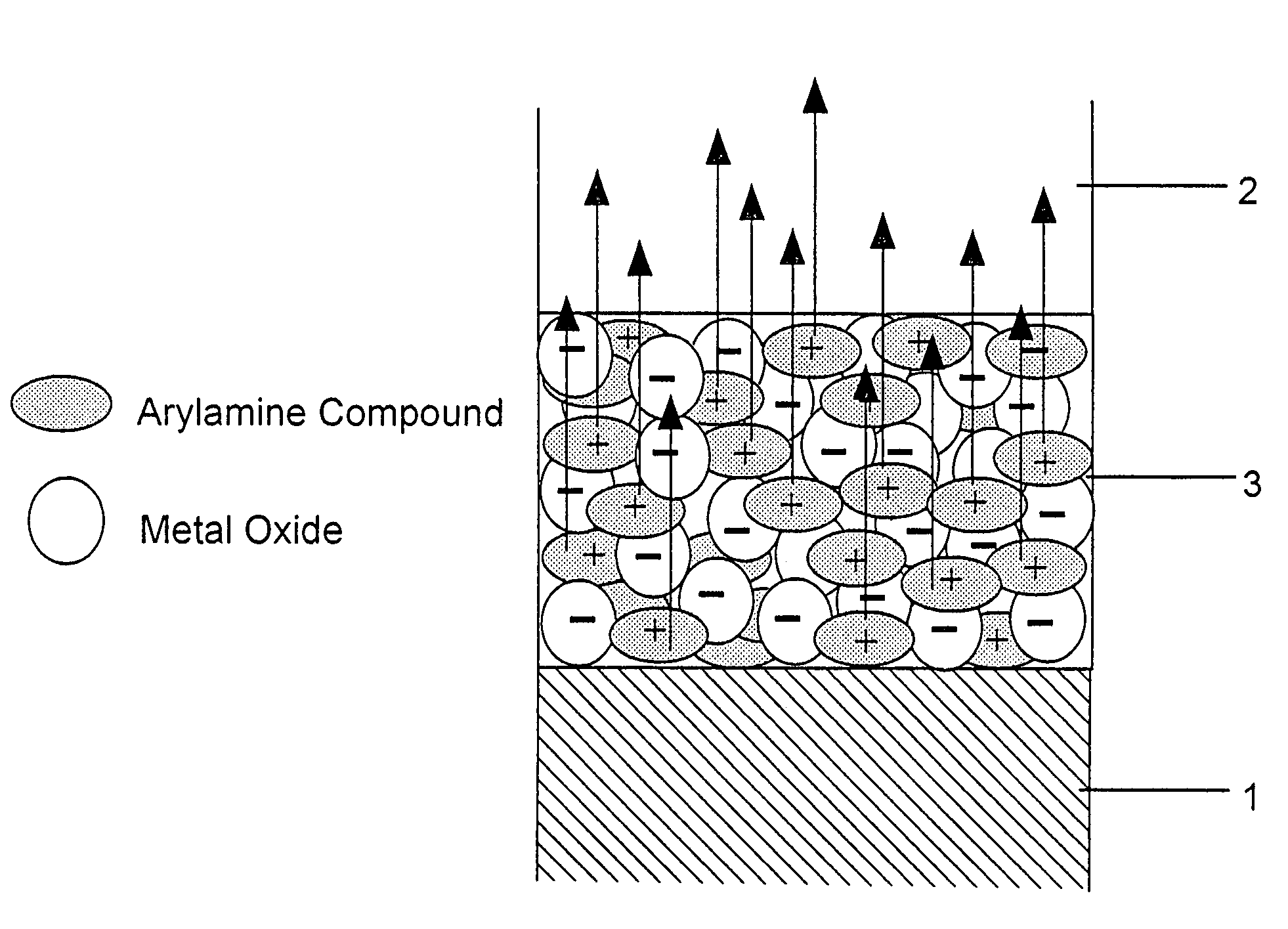
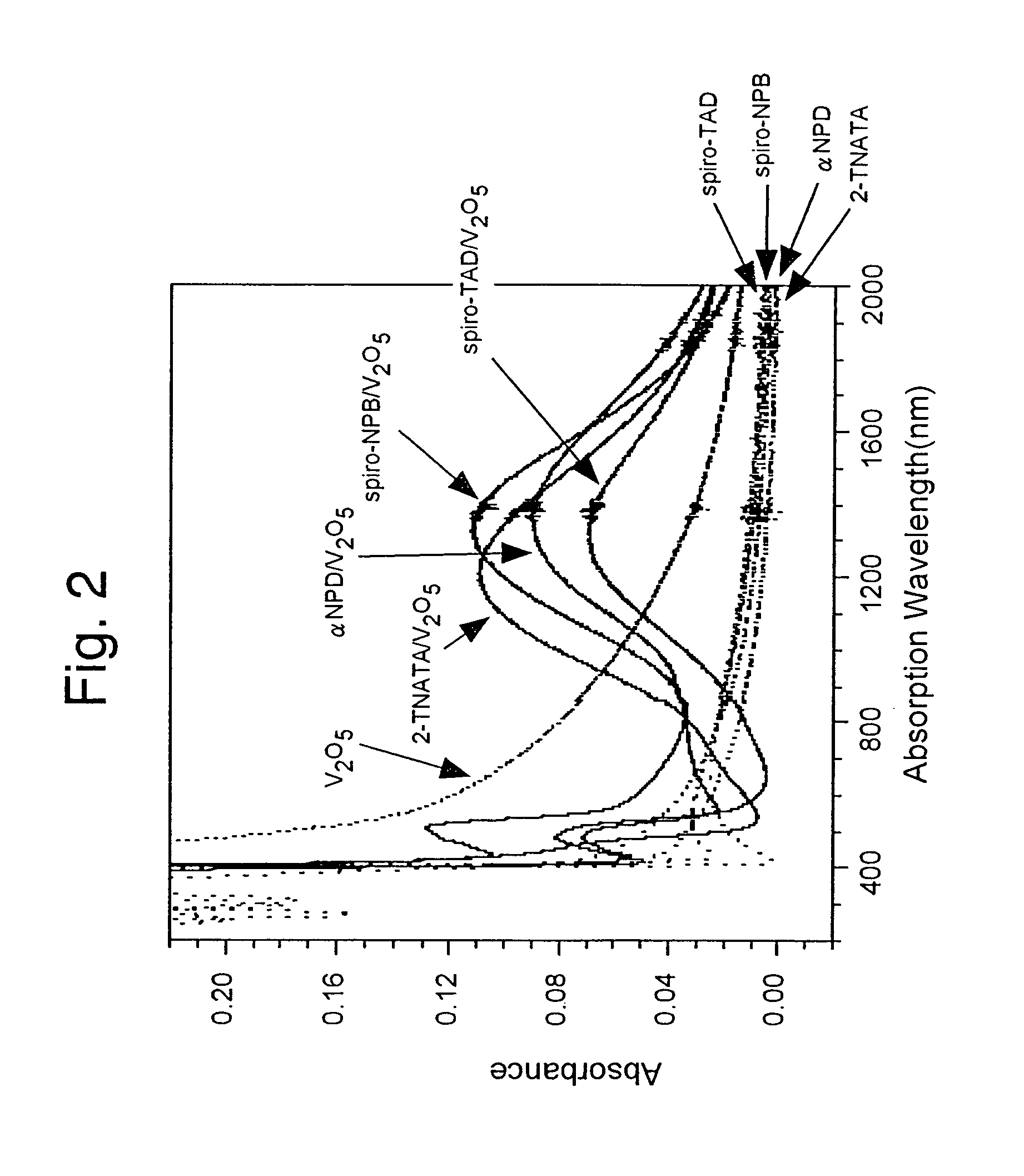
[0096]A glass substrate 21 is coated thereon with an ITO (indium-tin oxide; Nippon Sheet Glass Co., Ltd.) having a sheet resistance of about 10Ω / □ as a transparent anode electrode layer (anode electrode layer) 22. A metal oxide, V2O5, and an organic compound having a hole transporting property, α-NPD, are co-deposited at a molar ratio of V2O5:α-NPD of about 4:1 on the ITO-coated glass substrate 21 to form a mixed layer 27 having a thickness of about 100 Å acting as a hole injection layer.

[0097]Thereafter, a hole transportation layer (α-NPD) 23, a light-emissive layer (Alq) 24, an electron injection layer (metal doping layer, low resistance electron transportation layer) 25 and a cathode electrode layer (cathode) 26 are sequentially laminated as in the production of the EL device of the above-described Reference Example. Note that an organic structure 28 including a light-emissive lay...

example 2

[0099]In this example, the organic EL device having the lamination structure of FIG. 6 is fabricated.

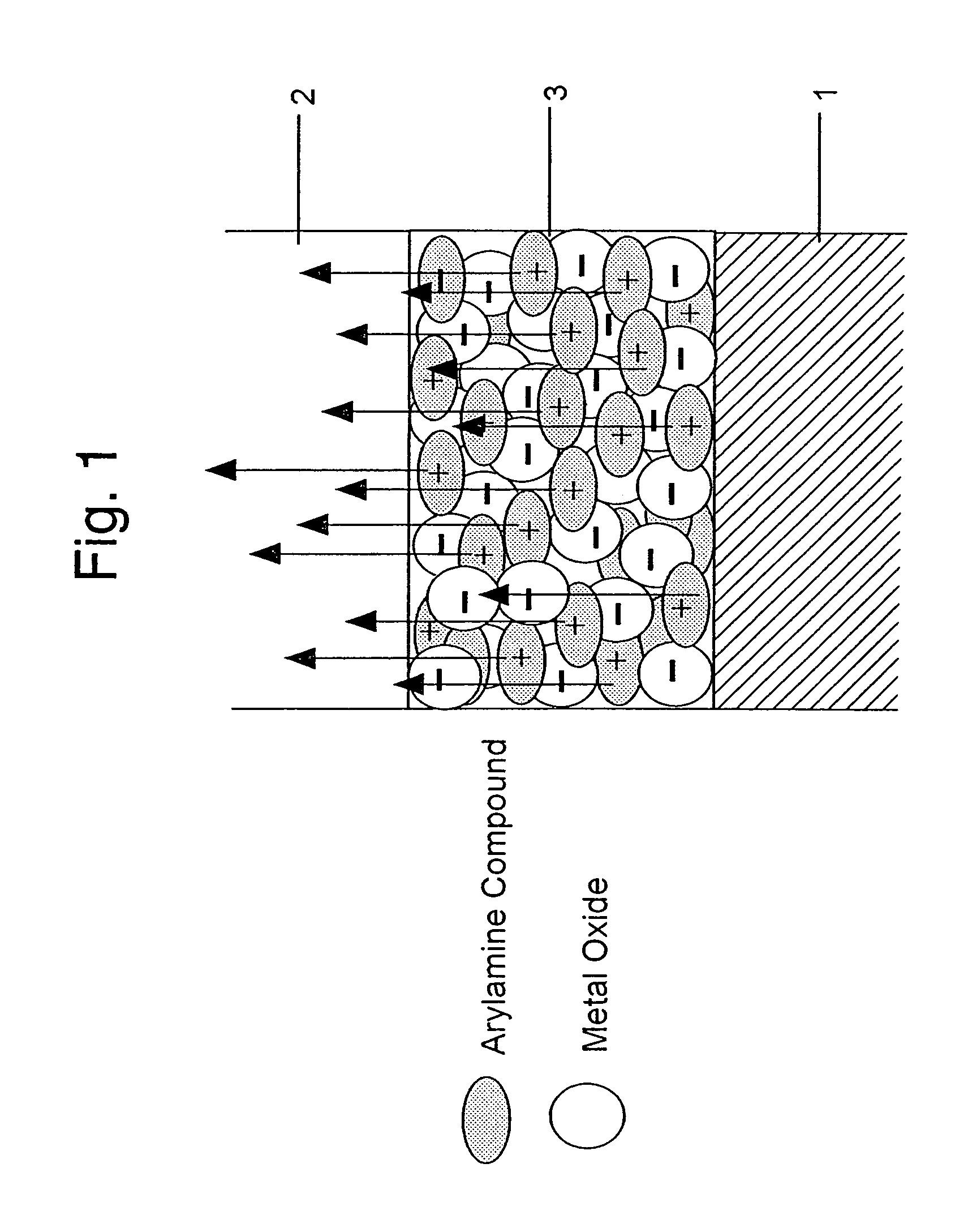
[0100]A glass substrate 31 is coated thereon with an ITO (indium-tin oxide; Nippon Sheet Glass Co., Ltd.) having a sheet resistance of about 10Ω / □ as a transparent anode electrode layer 32. A metal oxide, V2O5, and an organic compound having a hole transporting property, α-NPD, are co-deposited at a molar ratio of about 4:1 on the ITO-coated glass substrate 31 to form a mixed layer 37 having a thickness of about 1,000 Å acting as a hole injection layer of the present invention.

[0101]Thereafter, a hole transportation layer (α-NPD) 33, a light-emissive layer (Alq) 34, an electron injection layer (metal doping layer) 35 and a cathode electrode layer 36 are sequentially laminated as in the fabrication of the EL device of the above-described Reference Example. Note that an organic structure 38 including a light-emissive layer is formed from the hole transportation layer 33, the light-emis...

example 3

[0107]In this example, the organic EL device having the top emission structure of FIG. 12 is fabricated. An aluminum (Al; work function of about 4.2 eV) is deposited at the deposition rate of about 10 Å / sec under the pressure of about 10−6 Torr (1 Torr=133.32 Pa) (hereinafter, all deposition process is conducted under the same condition) on a glass substrate 41 to form an anode electrode layer 42 having a thickness of about 1,000 Å. A metal oxide, V2O5, and an organic compound having a hole transporting property, α-NPD, are co-deposited at a molar ratio of about 4:1 on an anode electrode layer 42 to form a mixed layer 47 having a thickness of about 100 Å acting as a hole injection layer of the present invention. Thereafter, α-NPD is deposited at the deposition rate of about 2 Å / sec on the hole injection layer 47 to form a hole transporting layer 43 having a thickness of about 600 Å. Subsequently, Alq is deposited on the hole transportation layer 43 under the same vapor deposition co...


PUM

PropertyMeasurementUnit
thicknessaaaaaaaaaa
ionization potentialaaaaaaaaaa
glass transition temperatureaaaaaaaaaa

Abstract

An organic electroluminescent device includes an anode electrode layer; a cathode electrode layer opposed to the anode electrode layer; a hole injection layer provided adjacent to the anode electrode layer an organic structure including at least one light-emissive layer or at least one light-emissive unit having at least one light-emissive layer; between the anode electrode layer and the cathode electrode layer. At least one of the anode electrode layer and the cathode electrode layer is transparent. The hole injection layer includes a mixed layer of a metal oxide and an organic compound. The mixed layer is formed upon co-deposition of the metal oxide and the organic compound.

Description

CROSS REFERENCE TO RELATED APPLICATION[0001]The present application is related to and claims priority of the following priority application, namely, Japanese patent application number 2003-358402 filed on Oct. 17, 2003 and incorporates by reference said priority application herein.BACKGROUND OF THE INVENTION[0002]1. Field of the Invention[0003]The present invention relates to an organic electroluminescent device (hereinafter, abbreviated as an “organic EL device”) which can be used as a planar light source or as a display device.[0004]2. Description of the Related Art[0005]Attention has been made to an organic electroluminescent device in which a light-emissive layer is constituted from an organic compound, because such a device can ensure a large area display at a low driving voltage. To highly increase the efficiency of organic EL devices, Tang et al. of Eastman Kodak Company, as is disclosed in Appl. Phys. Lett., 51, 913 (1987), have successfully achieved an EL device which can e...

Claims


Application Information

Patent Timeline
Patent Type & Authority Patents(United States)
IPC IPC(8): H01L51/50C09K11/06H01L51/00H01L51/30H05B33/14
CPCH01L51/5088H01L51/0052H01L51/0059H01L51/0077H01L51/0081H01L51/0062H10K85/649H10K85/615H10K85/631H10K85/30H10K85/324H10K50/17C09K11/06H05B33/14
Inventor KIDO, JUNJIMATSUMOTO, TOSHIONAKADA, TAKESHIKAWAMURA, NORIFUMI
Owner MITSUBISHI HEAVY IND LTD
Why Eureka
Try Eureka