Optoelectronic device employing a microcavity including a two-dimensional carbon lattice structure

a technology of optoelectronic devices and microcavities, applied in the direction of electric variable regulation, process and machine control, instruments, etc., can solve the problems of limited switching speed large device footprint of current optoelectronic devices based on silicon and group iii-v semiconductor compounds, and inability to operate in the terahertz regim

Active Publication Date: 2013-12-17
INT BUSINESS MASCH CORP +2
View PDF18 Cites 25 Cited by
  • Summary
  • Abstract
  • Description
  • Claims
  • Application Information

AI Technical Summary

Benefits of technology

[0005]A microcavity-controlled two-dimensional carbon lattice structure device selectively modifies to reflect or to transmit, or emits, or absorbs, electromagnetic radiation depending on the wavelength of the electromagnetic radiation. The microcavity-controlled two-dimensional carbon lattice structure device employs a graphene layer or at least one carbon nanotube located within an optical center of a microcavity defined by a pair of partial mirrors that partially reflect electromagnetic radiation. The spacing between the mirrors determines the efficiency of elastic and inelastic scattering of electromagnetic radiation inside the microcavity, and hence, determines a resonance wavelength of electronic radiation that is coupled to the microcavity. The resonance wavelength is tunable by selecting the dimensional and material parameters of the microcavity. The process for manufacturing this device is compatible with standard complementary metal oxide semiconductor (CMOS) manufacturing processes.

Problems solved by technology

Current optoelectronic technologies based on silicon and group III-V semiconductor compounds have large device footprints.
Further, current optoelectronic devices also have a limited switching speed.
For example, on-chip optoelectronic components operating in the terahertz regime are not currently available.
Despite the superior performance potential of a graphene layer and a carbon nanotube relative to silicon and group III-V semiconductor compounds in terms of such properties, formation of a compact optoelectronic device based on a graphene layer or a carbon nanotube and smaller than currently available optoelectronic technologies based on silicon and group III-V semiconductor compounds is a significant challenge because coupling between electromagnetic radiation and charge carriers of the graphene layer and / or the carbon nanotube is relatively weak.

Method used


Image

  • Optoelectronic device employing a microcavity including a two-dimensional carbon lattice structure
  • Optoelectronic device employing a microcavity including a two-dimensional carbon lattice structure
  • Optoelectronic device employing a microcavity including a two-dimensional carbon lattice structure

Examples


first embodiment

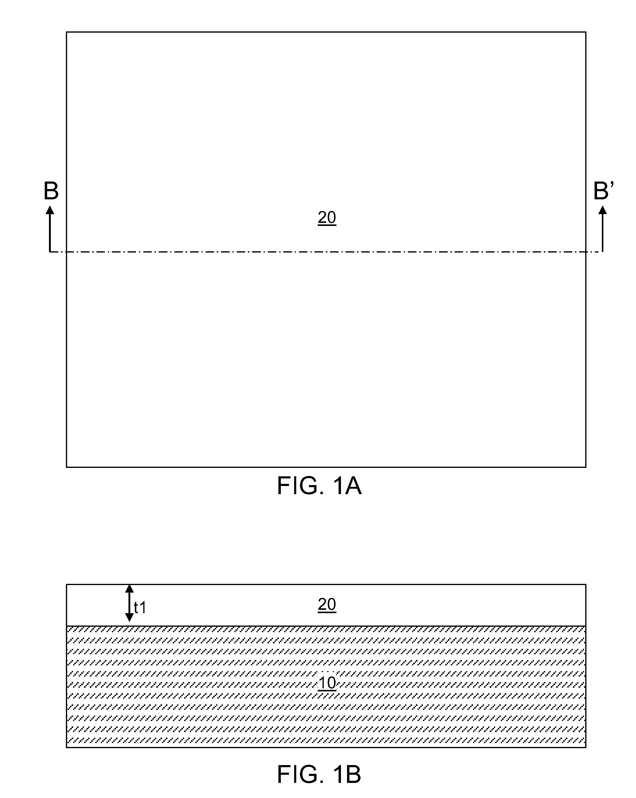
[0043]Referring to FIGS. 1A and 1B, a first exemplary structure according to the present disclosure includes a substrate 10. The substrate 10 can include a conductive material, an insulator material, a semiconductor material, or any solid material provided that the substrate 10 can provide structural support to layers to be subsequently formed.

[0044]A first transparent layer 20 having a first thickness t1 is formed on the top surface of the substrate 10. The first transparent layer 20 includes a material that is optically transparent within a wavelength range, which is herein referred to as a first transparent wavelength range. The first transparent layer 20 can be formed, for example, by chemical vapor deposition, physical vapor deposition, vacuum evaporation or evaporation at subatomic pressure, atomic layer deposition, spin coating, layer transfer and bonding from another substrate, or a combination thereof. The first transparent layer 20 has a first refractive index of n1.

[0045]...

third embodiment

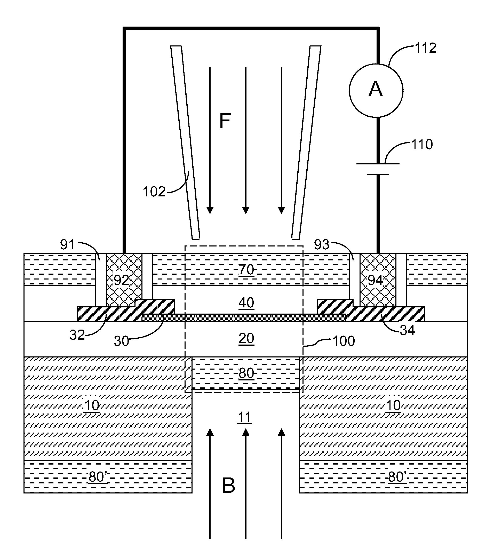
[0093]Referring to FIG. 13, the first bias and switching circuit of the third exemplary structure can be replaced with a second bias and switching circuit to provide a fourth exemplary structure. In the second bias and switching circuit, the DC voltage bias source 130 in the first bias and switching circuit is replaced with an alternating current voltage bias source 140, which applies an alternating current (AC) voltage bias across the at least one graphene layer 30 instead of a DC voltage bias. The amplitude of the AC voltage bias can be from 0.1 V to 100 V, and the frequency of the AC voltage bias can be from 1 Hz to 1 THz, although lesser and greater amplitudes and frequencies can also be employed. The fourth exemplary structure can be employed as an electromagnetic radiation emitter as in the

[0094]Referring to FIG. 14, a fifth exemplary structure is derived from the first exemplary structure of FIGS. 9A and 9B by connecting a bias and signal amplification circuit. The bias and s...

sixth embodiment

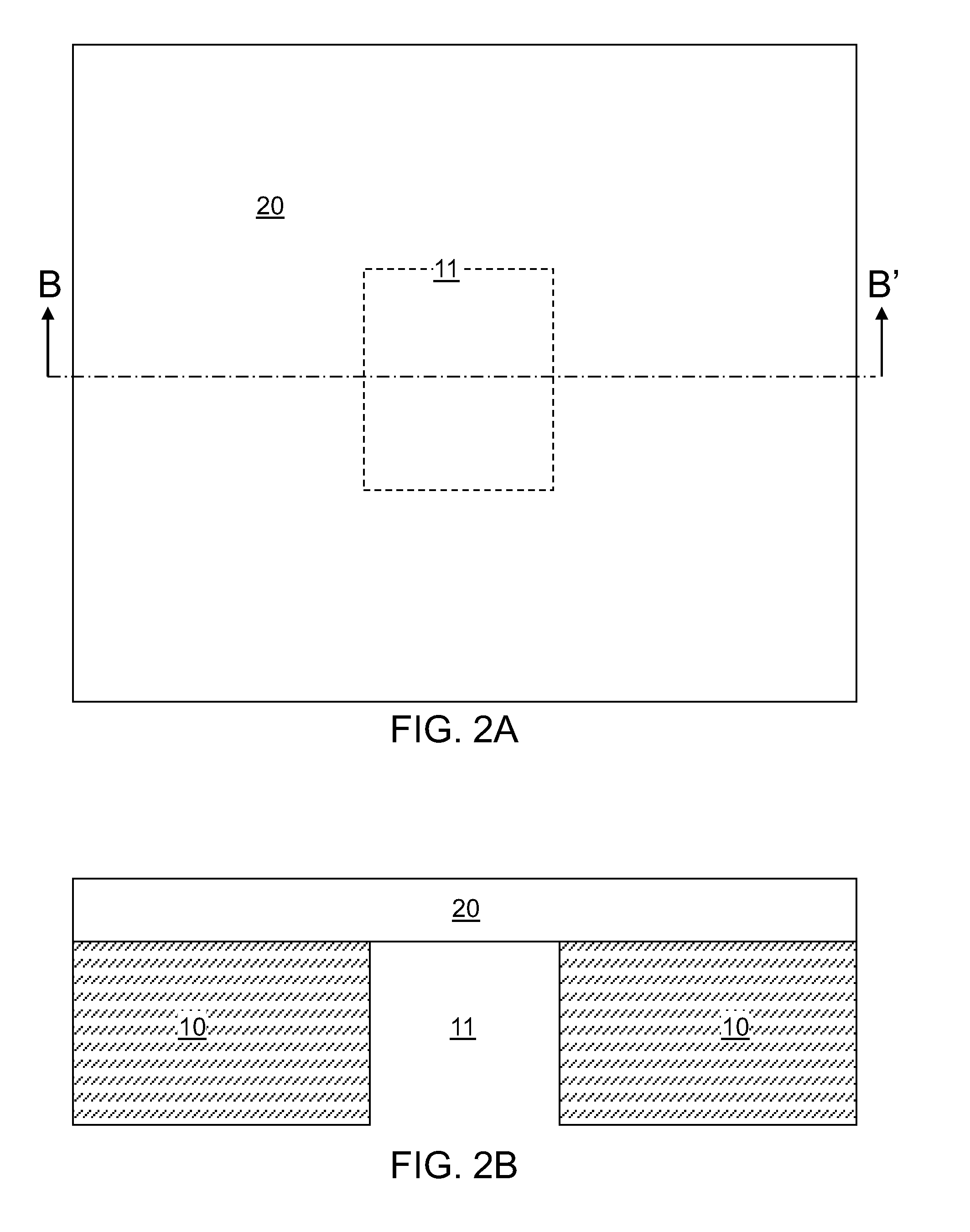
[0098]Referring to FIGS. 15A and 15B, a sixth exemplary structure according to the present disclosure can be derived from the first exemplary structure of FIGS. 2A and 2B by placing at least one carbon nanotube 230 on the first transparent layer 20 in lieu of at least one graphene layer 30. If the at least one carbon nanotube 230 is a plurality of carbon nanotubes, the plurality of carbon nanotubes can be aligned employing any method known in the art. Subsequently, processing steps of FIGS. 4A, 4B, 5A, 5B, 6A, 6B, 7A, and 7B can be performed to provide the sixth exemplary structure illustrated in FIGS. 16A and 16B.

[0099]Processing steps of FIGS. 8A, 8B, 9A, 9B, and 10 can be subsequently performed to provide the sixth exemplary structure of FIG. 17. The sixth exemplary structure of FIG. 17 is an electromagnetic radiation detector having the same operational principle as the electromagnetic radiation detector of FIG. 10 except for the difference of employing at least one carbon nanot...


PUM

PropertyMeasurementUnit
refractive index n1aaaaaaaaaa
thickness t1aaaaaaaaaa

Abstract

A microcavity-controlled two-dimensional carbon lattice structure device selectively modifies to reflect or to transmit, or emits, or absorbs, electromagnetic radiation depending on the wavelength of the electromagnetic radiation. The microcavity-controlled two-dimensional carbon lattice structure device employs a graphene layer or at least one carbon nanotube located within an optical center of a microcavity defined by a pair of partial mirrors that partially reflect electromagnetic radiation. The spacing between the mirror determines the efficiency of elastic and inelastic scattering of electromagnetic radiation inside the microcavity, and hence, determines a resonance wavelength of electronic radiation that is coupled to the microcavity. The resonance wavelength is tunable by selecting the dimensional and material parameters of the microcavity. The process for manufacturing this device is compatible with standard complementary metal oxide semiconductor (CMOS) manufacturing processes.

Description

BACKGROUND[0001]The present disclosure relates to an optoelectronic device, and particularly to an optoelectronic device employing a microcavity and a two-dimensional lattice structure embedded therein, and methods of manufacturing the same.[0002]Current optoelectronic technologies based on silicon and group III-V semiconductor compounds have large device footprints. For example, typical optoelectronic devices currently available have an average device area on the order of a square millimeter. Further, current optoelectronic devices also have a limited switching speed. For example, on-chip optoelectronic components operating in the terahertz regime are not currently available.[0003]Two-dimensional carbon lattice structures include sp2-bonded carbon atoms that are densely packed in a hexagonal lattice structure. If the two-dimensional carbon lattice structure is topologically planar, the two-dimensional carbon lattice structure constitutes a graphene layer. If the two-dimensional car...

Claims


Application Information

Patent Timeline
Patent Type & Authority Patents(United States)
IPC IPC(8): G02F1/03G02F1/00H01L27/14
CPCB82Y20/00H01L31/0352B82Y10/00H01L51/0048H10K85/221
Inventor AVOURIS, PHAEDONSTEINER, MATHIAS B.ENGEL, MICHAELKRUPKE, RALPHFERRARI, ANDREA C.LOMBARDO, ANTONIO
Owner INT BUSINESS MASCH CORP
Why Eureka
Try Eureka