Method for focused electric-field imprinting for micron and sub-micron patterns on wavy or planar surfaces

a focused electric field and micro- and sub-micron pattern technology, applied in the field of semiconductor manufacturing, can solve the problems of lithographic based fabrication facilities, high cost of ownership (coo), and the inability to meet the requirements of miniaturized components, and achieves the effect of easy control and scalabl

a focused electric field and micro- and sub-micron pattern technology, applied in the field of semiconductor manufacturing, can solve the problems of lithographic based fabrication facilities, high cost of ownership (coo), and the inability to meet the requirements of miniaturized components, and achieves the effect of easy control and scalabl

US8617378B1Inactive Publication Date: 2013-12-31ACTUS POTENTIA

Image

  • Method for focused electric-field imprinting for micron and sub-micron patterns on wavy or planar surfaces
  • Method for focused electric-field imprinting for micron and sub-micron patterns on wavy or planar surfaces
  • Method for focused electric-field imprinting for micron and sub-micron patterns on wavy or planar surfaces

Examples


Embodiment Construction

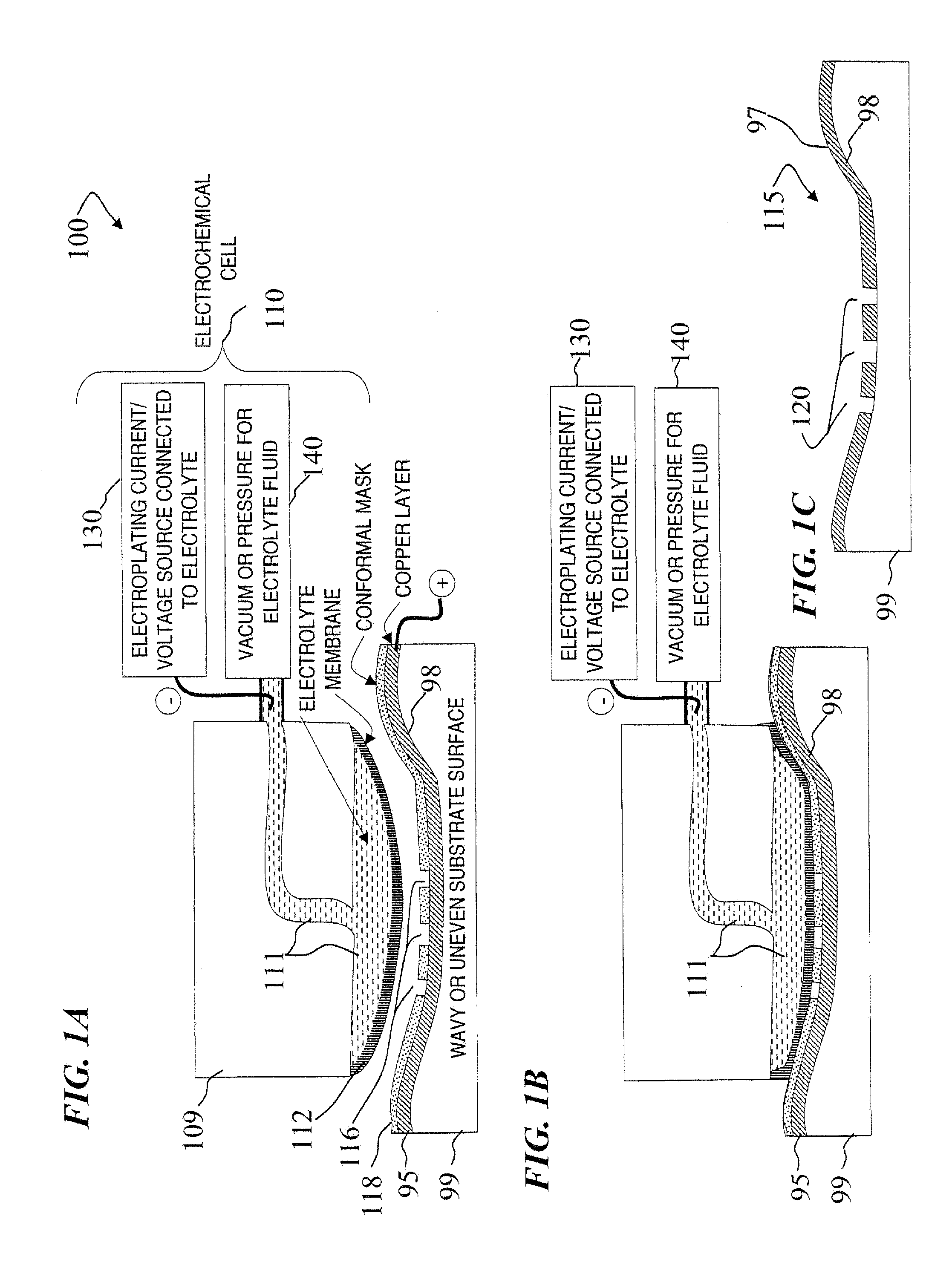
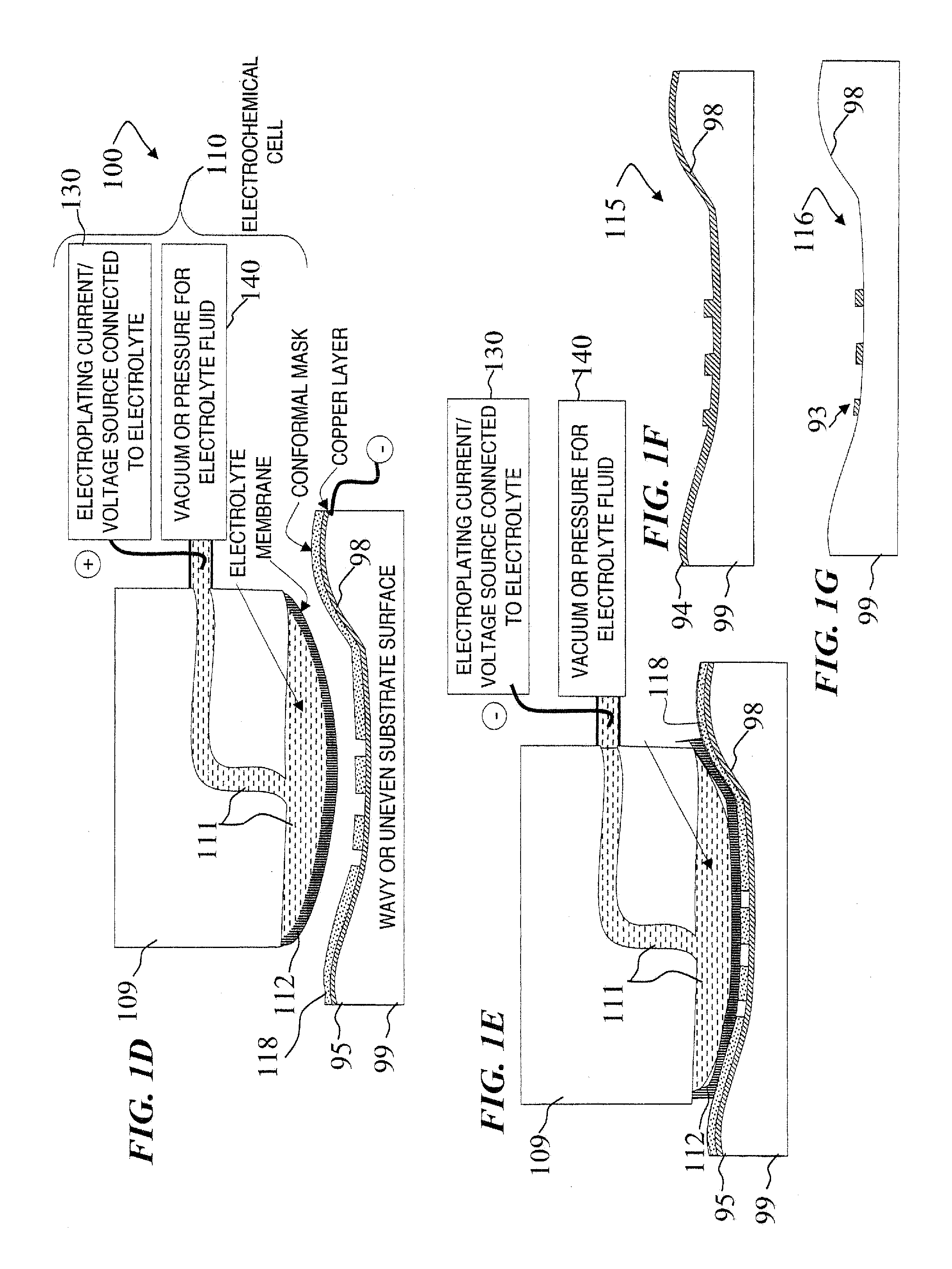
[0040]Although the following detailed description contains many specifics for the purpose of illustration, a person of ordinary skill in the art will appreciate that many variations and alterations to the following details are within the scope of the invention. Accordingly, the following preferred embodiments of the invention are set forth without any loss of generality to, and without imposing limitations upon the claimed invention. Further, in the following detailed description of the preferred embodiments, reference is made to the accompanying drawings that form a part hereof, and in which are shown by way of illustration specific embodiments in which the invention may be practiced. It is understood that other embodiments may be utilized, and that structural, sequential, and temporal changes may be made without departing from the scope of the present invention.

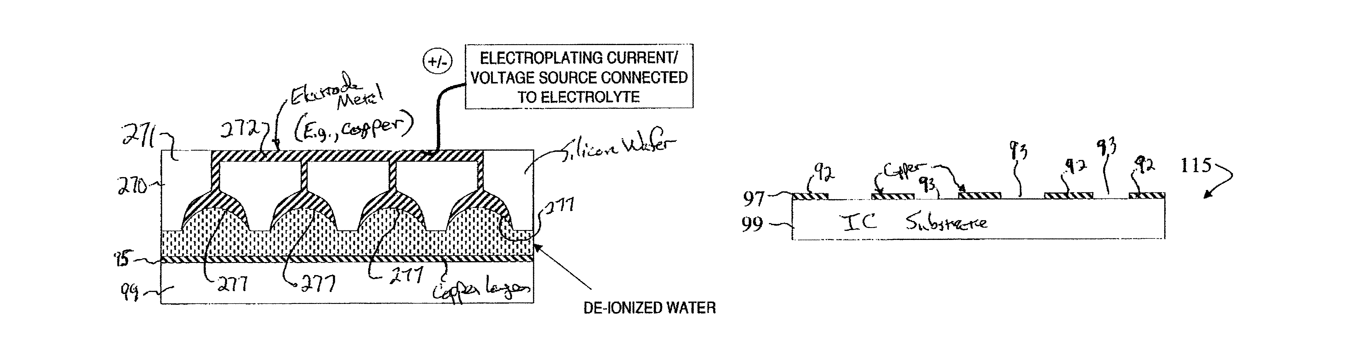
[0041]The leading digit(s) of reference numbers appearing in the Figures generally corresponds to the Figure number in wh...


PUM

PropertyMeasurementUnit
widthaaaaaaaaaa
smoothnessaaaaaaaaaa
thicknessaaaaaaaaaa

Abstract

Focused Electric Field Imprinting (FEFI) provides a focused electric field to guide an unplating operation and / or a plating operation to form very fine-pitched metal patterns on a substrate. The process is a variation of the electrochemical unplating process, wherein the process is modified for imprinting range of patterns of around 2000 microns to 20 microns or less in width, and from about 0.1 microns or less to 10 microns or more in depth. Some embodiments curve a proton-exchange membrane whose shape is varied using suction on a backing fluid through a support mask. Other embodiments use a curved electrode. Mask-membrane interaction parameters and process settings vary the feature size, which can generate sub-100-nm features. The feature-generation process is parallelized, and a stepped sequence of such FEFI operations, can generate sub-100-nm lines with sub-100-nm spacing. The described FEFI process is implemented on copper substrate, and also works well on other conductors.

Description

CROSS-REFERENCE TO RELATED APPLICATION[0001]This application is a divisional of U.S. patent application Ser. No. 11 / 811,288, filed on Jun. 7, 2007, titled “METHOD AND APPARATUS FOR FOCUSED ELECTRIC-FIELD IMPRINTING FOR MICRON AND SUB-MICRON PATTERNS ON WAVY OR PLANAR SURFACES” (which issued as U.S. Pat. No. 7,998,323 on Aug. 16, 2011), which claimed benefit under 35 U.S.C. 119(e) of U.S. Provisional Patent Application No. 60 / 804,163, filed on Jun. 7, 2006, titled “METHOD AND APPARATUS FOR FOCUSED ELECTRIC-FIELD IMPRINTING FOR MICRON AND SUB-MICRON PATTERNS ON WAVY OR PLANAR SURFACES,” each of which is incorporated herein by reference in its entirety.FIELD OF THE INVENTION[0002]The invention relates to the field of semiconductor manufacturing, and more specifically, the invention describes a new technique for electrochemical unplating or plating / deposition of micro and nano-scale patterns. The invention describes a procedure that is a potential substitute for lithography.BACKGROUND O...

Claims


Application Information

Patent Timeline
31 Dec 2013
Publication
US8617378B1
IPC
B23H3/00; C25D5/02
CPC
C25D17/00; C25F3/14; C25F3/02; C25D5/22; C25D5/02
Inventors
MITRA, AMBAR K.; BASTAWROS, ASHRAF F.