Manufacturing method of semiconductor device
a manufacturing method and semiconductor technology, applied in semiconductor devices, chemical vapor deposition coatings, coatings, etc., can solve problems such as reliability reduction, and achieve the effects of high etching selectivity, high accuracy, and reduced etching of oxide semiconductor layers
- Summary
- Abstract
- Description
- Claims
- Application Information
AI Technical Summary
Benefits of technology
Problems solved by technology
Method used
Image

Examples
embodiment 1
(Embodiment 1)
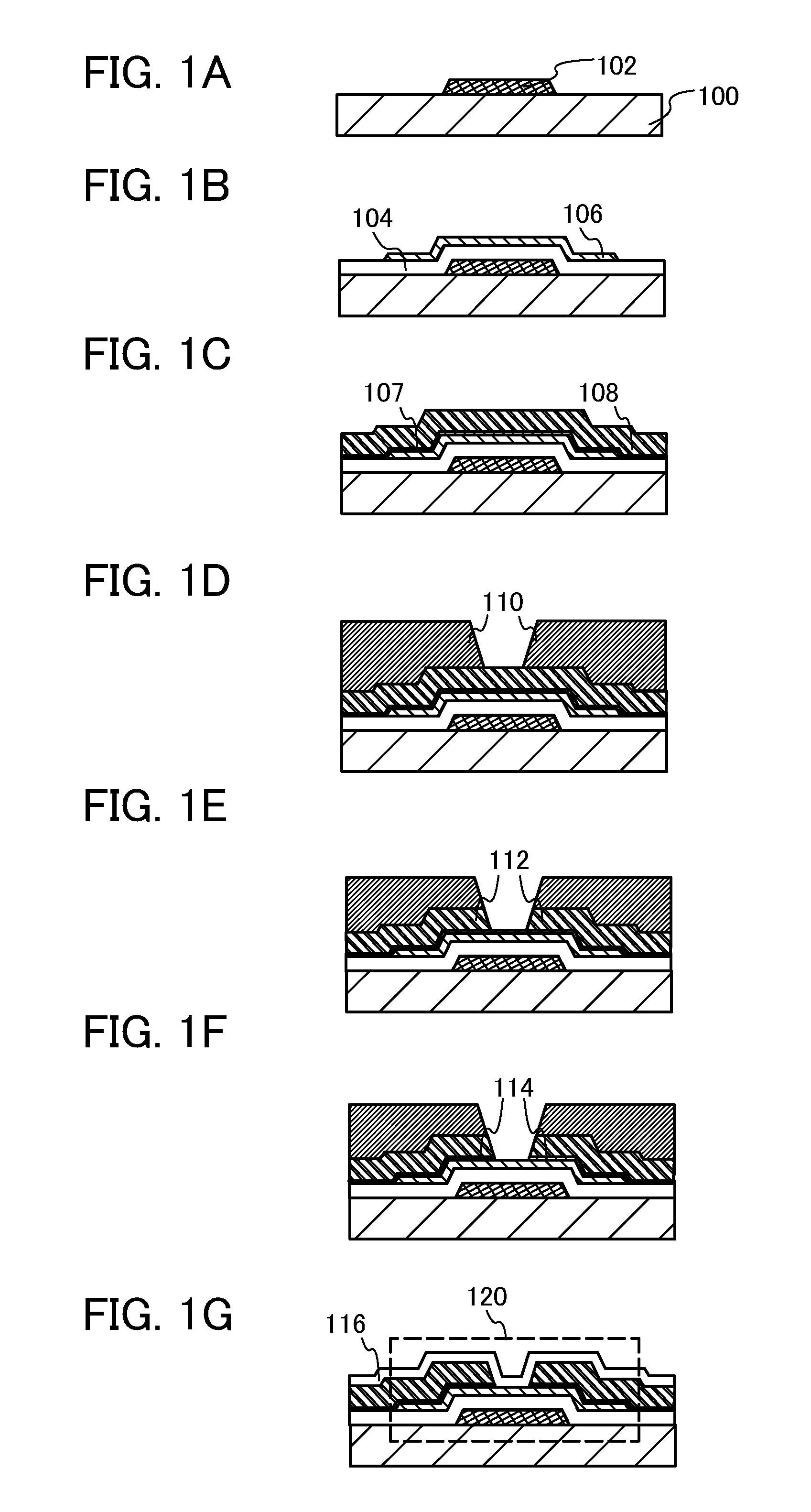
[0045]In this embodiment, a manufacturing method of a semiconductor device including a transistor according to an embodiment of the present invention will be described.
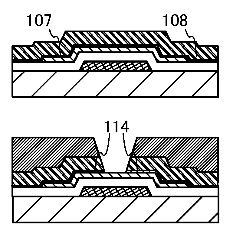
[0046]First, a gate electrode layer 102 is selectively formed over a substrate 100 (see FIG. 1A).
[0047]The substrate 100 may have an insulating surface. For example, a glass substrate, a quartz substrate, a semiconductor substrate having an insulating layer formed on its surface, or a stainless steel substrate having an insulating layer formed on its surface may be used.
[0048]The gate electrode layer 102 may be formed using a conductive material. A conductive material film to be the gate electrode layer 102 is formed and processed by a photolithography method.
[0049]A gate insulating film 104 is formed to cover the gate electrode layer 102, and an oxide semiconductor layer 106 is selectively formed over the gate insulating film 104 (see FIG. 1B).
[0050]The gate insulating film 104 is preferably formed usin...
embodiment 2
(Embodiment 2)
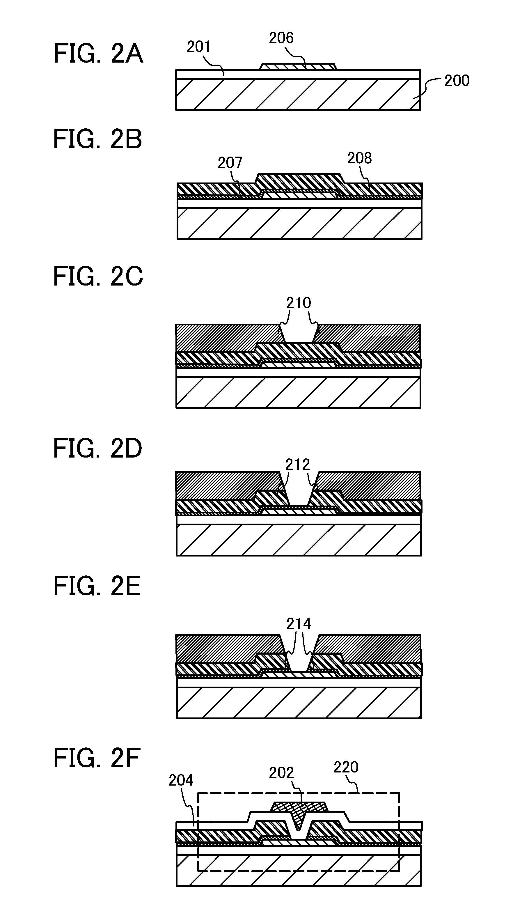
[0120]The present invention is not limited to the description in Embodiment 1. For example, a semiconductor device disclosed in this specification may have a top-gate structure in which a gate electrode layer is provided over a wiring layer.
[0121]First, a base insulating layer 201 is preferably formed over a substrate 200, and an oxide semiconductor layer 206 is selectively formed over the base insulating layer 201 (see FIG. 2A).
[0122]The substrate 200 may be the same as the substrate 100 in Embodiment 1.
[0123]The base insulating layer 201 can be formed using a material and a method similar to those of the gate insulating film 104 or the like in Embodiment 1.
[0124]The oxide semiconductor layer 206 can be formed using a material and a method similar to those of the oxide semiconductor layer 106 in Embodiment 1.
[0125]Next, a protective conductive film 207 is formed to cover the base insulating layer 201 and the oxide semiconductor layer 206, and a conductive layer 208 to...
embodiment 3
(Embodiment 3)
[0142]In this embodiment, the appearance and a cross section of a liquid crystal display panel, which corresponds to one embodiment of a semiconductor device, will be described with reference to FIGS. 3A to 3C. The liquid crystal display panel illustrated in FIGS. 3A to 3C includes the transistor described in Embodiment 1; however, the liquid crystal display can include the transistor described in any of Embodiments 1 and 2. FIGS. 3A and 3C are plan views of panels in each of which a transistor 4010, a transistor 4011, and a liquid crystal element 4013 are sealed between a first substrate 4001 and a second substrate 4006 with a sealant 4005. FIG. 3B is a cross-sectional view taken along the line M-N in FIG. 3A or FIG. 3C.
[0143]The sealant 4005 is provided to surround a pixel portion 4002 and a scan line driver circuit 4004 which are provided over the first substrate 4001. The second substrate 4006 is provided over the pixel portion 4002 and the scan line driver circuit...
PUM
| Property | Measurement | Unit |
|---|---|---|
| thickness | aaaaa | aaaaa |
| temperature | aaaaa | aaaaa |
| thickness | aaaaa | aaaaa |
Abstract
Description
Claims
Application Information
 - Generate Ideas
- Intellectual Property
- Life Sciences
- Materials
- Tech Scout
- Unparalleled Data Quality
- Higher Quality Content
- 60% Fewer Hallucinations
Browse by: Latest US Patents, China's latest patents, Technical Efficacy Thesaurus, Application Domain, Technology Topic, Popular Technical Reports.
© 2025 PatSnap. All rights reserved.Legal|Privacy policy|Modern Slavery Act Transparency Statement|Sitemap|About US| Contact US: help@patsnap.com