Non-polar ultraviolet light emitting device and method for fabricating same

a technology of non-polar ultraviolet light and light emitting device, which is applied in the manufacture of semiconductor/solid-state devices, semiconductor devices, electrical devices, etc., can solve the problems of difficult manufacturing of ultraviolet emitting leds, formation of crystalline defects, and lattice and thermal mismatch between defects, etc., to achieve the effect of improving ultraviolet emitting leds

Active Publication Date: 2014-04-01
NIITEK
View PDF12 Cites 6 Cited by
  • Summary
  • Abstract
  • Description
  • Claims
  • Application Information

AI Technical Summary

Benefits of technology

[0014]The present diode demonstrates a reduced defect density when a group III-Nitride epitaxial layer is used in conjunction with a patterned template, where the template consists of a patterned non c-plane substrate with a single or multi-layer first buffer of III-Nitride semiconductor layers that are optionally etched into pillars. The low defect density III-Nitride second buffer layer is formed thereover by using a pulsed lateral overgrown III-Nitride layer.
[0016]A feature of the present invention is that the buffer layer of the present invention can be either a single III-Nitride layer that is not thin (thickness >0.1 μm) for AlN, or consist of ternary (AlGaN, AlInN), quaternary (AlInGaN) or multiple layers of III-Nitride, preferably made of AlInGaN containing less than 0.2 mole fraction indium and containing a design optimized for both strain relief and optical transparency. In the prior art, the buffer layer consists of thin AlN in a single layer. Another feature is the use of the superlattice for both reducing defects and relieving strain. A superlattice is a series of thin layers of alternating composition that serves as a transducer from a lower layer to an upper layer, relieving stress and shifting the intralattice geometry from the first to the second layer.
[0017]Another feature of the present invention is the formation of deep trenches (depth ≧0.1 μm) before performing the PLOG growth. This shallow etch depth limited the amount of lateral overgrowth that could be successfully performed because growth also takes place in the trenches. In the present invention, the pillars can consist of either a non-c plane oriented single AlInGaN layer, or non-c plane oriented multiple stacks of AlInGaN layers with the etch depth greater than or equal to 0.1 μm, including any etching that occurs into the substrate.

Problems solved by technology

UV emitting LED's are difficult to manufacture for a number of reasons.
For example, defects arise from lattice and thermal mismatch between the group III-Nitride based semiconductor layers and the substrate.
In addition, impurities and tilt boundaries result in the formation of crystalline defects.
These defects have been shown to reduce the efficiency and lifetime of LEDs and LDs fabricated from these materials.
This method, however, has been shown to be ineffective for the growth of aluminum-containing III-Nitride based semiconductors because of the tendency for the aluminum to stick to the masked material and disrupt the lateral overgrowth.
All of these techniques suffer from the same limitation as the ELOG approach for aluminum containing III-Nitride materials.
The structure of the c-plane comprises a high density of threading dislocations which significantly reduces the lifetime of the light emitters and the manufacturing yield.
The consequent reduction in the envelope wave-function overlap results in a lower radiative efficiency for light-emitting devices.
While helpful, this problem has not proven satisfactory for UV LED's which require high aluminum containing AlInGaN quantum wells when conventional deposition techniques are used.
Under standard deposition conditions the epilayer quality suffers due to high gas phase reaction of the precursor sources.
In addition, high aluminum containing AlInGaN device structure cracks due to tensile stress when grown directly on GaN substrates.

Method used


Image

  • Non-polar ultraviolet light emitting device and method for fabricating same
  • Non-polar ultraviolet light emitting device and method for fabricating same
  • Non-polar ultraviolet light emitting device and method for fabricating same

Examples


Embodiment Construction

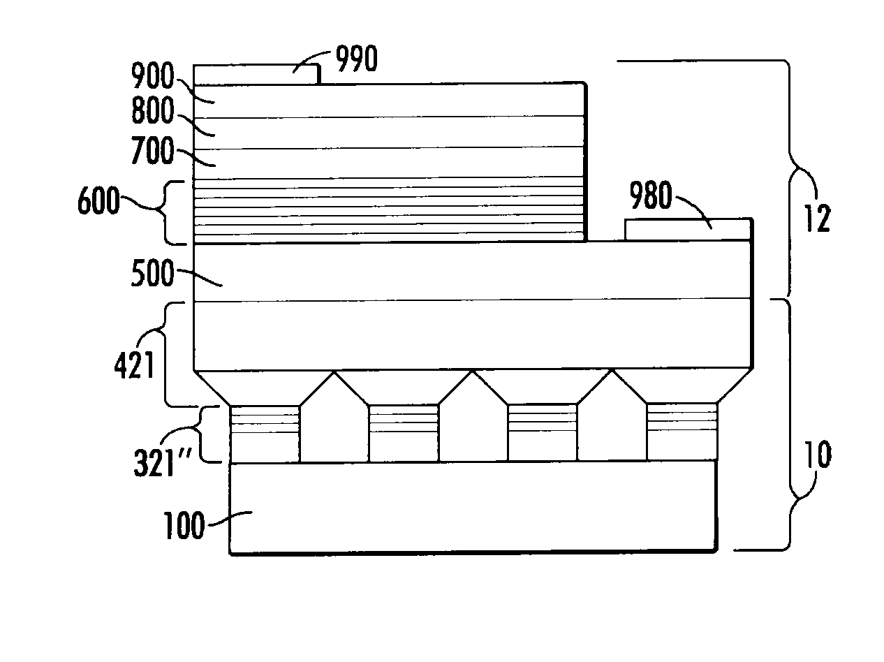
[0034]The present invention is an ultraviolet light-emitting device (LED) and a method for making an LED, particularly one that emits ultraviolet, and more preferably deep ultraviolet light. In particular, it is a template 10 that serves as a platform for an ultraviolet light-emitting structure 12 as shown in FIG. 4. Briefly, template 10 includes a non c-plane substrate. More preferably the substrate includes an m-plane {1-100} buffer layer, an a-plane {11-20} buffer layer, a {1014} semi polar buffer layer, a {1122} semi polar buffer layer, a {1011} semi polar buffer layer, a {1013} semi polar buffer layer, a {1012} semi polar buffer layer, and a {2021} semi polar buffer layer of a substrate with the m-plane and a-plane being more preferable and the m-plane being most preferable. The substrate is preferably selected from the group consisting of aluminum nitride, gallium nitride, aluminum gallium nitride, aluminum indium gallium nitride, aluminum indium nitride, SiC, sapphire and lit...


PUM


Abstract

An ultra-violet light-emitting device and method for fabricating an ultraviolet light emitting device, 12, (LED or an LD) with an AlInGaN multiple-quantum-well active region, 10, exhibiting stable cw-powers. The device includes a non c-plane template with an ultraviolet light-emitting structure thereon. The template includes a first buffer layer, 321, on a substrate, 100, then a second buffer layer, 421, on the first preferably with a strain-relieving layer, 302, in both buffer layers. Next there is a semiconductor layer having a first type of conductivity, 500, followed by a layer providing a quantum-well region, 600. Another semiconductor layer, 700, having a second type of conductivity is applied next. Two metal contacts, 980 and 990, are applied to this construction, one to the semiconductor layer having the first type of conductivity and the other to the semiconductor layer having the second type of conductivity, to complete the light emitting device.

Description

CROSS-REFERENCE TO RELATED APPLICATIONS[0001]The present application claims priority to U.S. Provisional Patent Application No. 60 / 924,289 filed May 8, 2007 which is incorporated herein by reference.BACKGROUND OF THE INVENTION[0002]The present invention relates generally to a non-polar ultraviolet light-emitting device and method of manufacturing a light-emitting device.[0003]Group III nitride compound semiconductors such as, for instance, gallium nitride (GaN), aluminum nitride (AlN), indium nitride (InN) (hereinafter also referred to as a “Group III-nitride semiconductor” or “III-nitrides”) have been gaining attention as a material for semiconductor devices that emit green, blue or ultraviolet light. A light-emitting device, which together with the acronym LED when used herein, will for convenience also refer to both a light-emitting diode and laser diode (LD) unless otherwise specified. Of particular interest herein are LED's which emit in the ultraviolet portion of the electroma...

Claims


Application Information

Patent Timeline
Patent Type & Authority Patents(United States)
IPC IPC(8): H01L33/16H01L33/12H01L33/32H01L31/00H01L29/06
CPCH01L21/0265H01L21/02378H01L33/32H01L21/0254H01L21/02516H01L21/02389H01L21/02639H01L21/02507H01L21/02458H01L21/02433H01L33/16H01L33/12H01L21/0242
Inventor KHAN, ASIF
Owner NIITEK
Why Eureka
Try Eureka