Electron microscope

a technology of electron microscope and electron microscope, which is applied in the direction of material analysis using wave/particle radiation, instruments, nuclear engineering, etc., can solve the problems of beam drift phenomenon, non-uniform charging potential on the sample surface, and various types of image degradation, so as to achieve the effect of minimizing blur

Active Publication Date: 2014-06-03
HITACHI HIGH-TECH CORP
View PDF18 Cites 1 Cited by
  • Summary
  • Abstract
  • Description
  • Claims
  • Application Information

AI Technical Summary

Benefits of technology

[0030]The structure according to the present invention is capable of providing an image with minimized blur by suppressing the beam drift generated through charging on the sample surface.

Problems solved by technology

Especially when observing the insulator sample, the electron beam radiation generates the secondary electron and the backscattered electron to charge the sample surface, resulting in various types of image degradation.
Especially, charging makes the potential on the sample surface non-uniform around the electron beam radiation point to generate potential gradient.
This may deflect the electron beam trajectory to cause the beam drift phenomenon and an accompanying image blur.
The aforementioned art is effective for the reticle observation, but is difficult to completely remove the influence of charging.
Especially for the sample which has the charging state largely changed depending on the incident beam energy, for example, the reticle having the surface coated with resist, stable measurement precision cannot be established.
However, the configuration disclosed in Patent Literature 2 significantly degrades the resolution, and does not disclose the specific configuration of the magnetic disc efficient for the charging reduction.
However, such effect is limited, and consideration with respect to resolution degradation is insufficient.

Method used


Image

  • Electron microscope
  • Electron microscope
  • Electron microscope

Examples


first embodiment

[0044]Embodiments of the present invention will be described referring to the drawings.

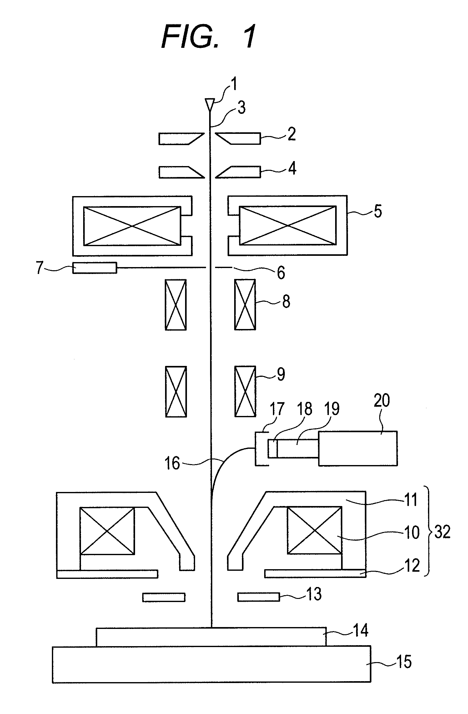
[0045]FIG. 1 is a schematic view of an electron microscope according to an embodiment. This embodiment is intended to conduct measurement and inspection of the interconnection on the wafer with respect to a large sample such as a semiconductor wafer under the condition where energy of a primary electron beam is set at low acceleration voltage ranging from several 100 eV to several keV. The present invention is applicable to the electron microscope irrespective of larger intended sample or object, and higher acceleration voltage so long as it has the similar structure.

[0046]When applying an extraction voltage between a field emission cathode 1 and an extraction electrode 2 as an electron source, an emitted electron 3 is released. The emitted electron 3 is further accelerated between the extraction electrode 2 and an anode 4 at a ground potential. Energy (acceleration voltage) of the electron beam p...

second embodiment

[0060]A second embodiment will be described referring to FIG. 9. The description of the first embodiment is applicable to this embodiment unless the circumstances are exceptional.

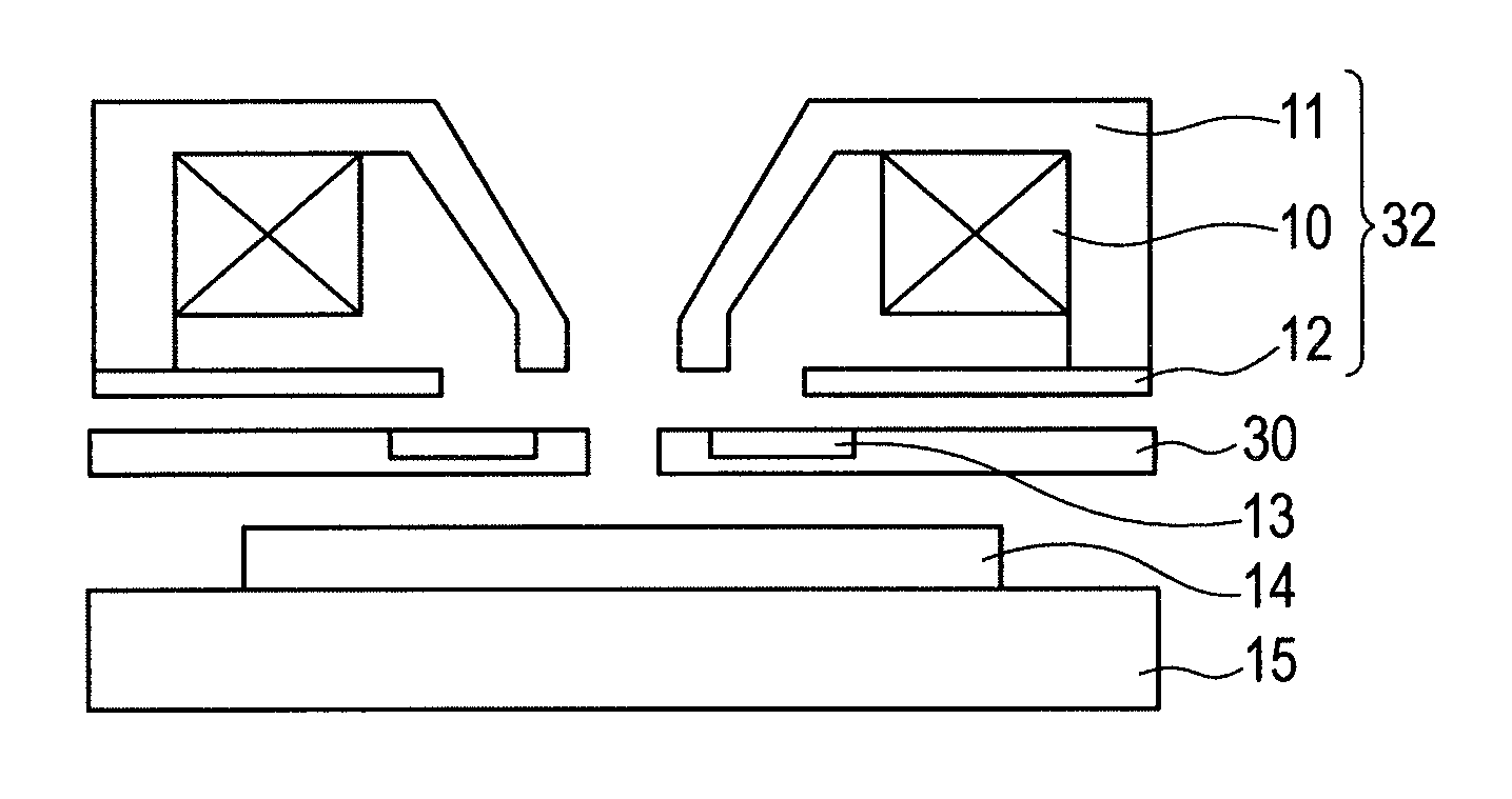
[0061]FIG. 9 illustrates a structure in which a non-magnetic body 30 is further disposed underneath the magnetic body 13 between the objective lens 32 and the sample 14. The sample 14 is held on the sample holder 15. The magnetic body 13 and the non-magnetic body 30 may be made conductive for the purpose of applying the same voltage, or may be insulated for the purpose of applying different voltage. The non-magnetic body 30 is disposed parallel to the sample holder 15, and is made larger than the magnetic body 13 so as to allow controlling of the potential on the sample surface. The non-magnetic body 30 functions to make it difficult to charge the insulating sample as well as suppress the beam drift by reducing the potential gradient on the sample surface.

[0062]FIGS. 10A and 10B schematically show equipoten...

third embodiment

[0065]In the second embodiment, the non-magnetic body is disposed underneath the magnetic body. Such structure increases a working distance between the objective lens and the sample, and the principal plane of the objective lens is far from the sample, thus degrading the resolution. The aforementioned problem may be solved by forming a trench in the non-magnetic body for storage of the magnetic body. FIGS. 13A and 13B illustrate the structure in which the trench is formed in the non-magnetic body for storage of the magnetic body. FIG. 13A illustrates that the trench is formed in the lower side of the non-magnetic body. FIG. 13B illustrates that the trench is formed in the upper side of the non-magnetic body. The structure having the magnetic body fit in the trench provides the advantage of suppressing the resolution degradation by reducing the working distance as well as improvement of the electrode positioning precision. In Embodiments 2 and 3, three electrodes (upper pole piece, m...


PUM


Abstract

A scanning electron microscope suppresses a beam drift by reducing charging on a sample surface while suppressing resolution degradation upon observation of an insulator sample. An electron microscope includes an electron source and an objective lens that focuses an electron beam emitted from the electron source, which provides an image using a secondary signal generated from the sample irradiated with the electron beam. A magnetic body with a continuous structure and an inside diameter larger than an inside diameter of an upper pole piece that forms the objective lens is provided between the objective lens and the sample.

Description

TECHNICAL FIELD[0001]The present invention relates to an electron microscope.BACKGROUND[0002]A scanning electron microscope is configured to accelerate electrons emitted from an electron source of thermal type or field emission type to form a thin electron beam (primary electron beam) using an electrostatic lens or a magnetic lens, subject the primary electron beam to two-dimensional scanning on a sample surface to be observed, detect a secondary signal, for example, secondary electron or backscattered electron secondarily generated from the sample resulting from radiation of the primary electron beam, and set the detected signal intensity to a brightness modulation input of a cathode-ray tube which is scanned simultaneously with scanning of the primary electron beam so as to provide a two-dimensional scan image. The use of the scanning electron microscope for the process of fabricating semiconductor devices or inspection after completion (for example, critical dimension measurement...

Claims


Application Information

Patent Timeline
Patent Type & Authority Patents(United States)
IPC IPC(8): H01J37/04H01J37/14H01J37/145
CPCH01J37/28H01J2237/153H01J37/04H01J37/145H01J2237/121H01J2237/0044H01J37/153H01J2237/004H01J37/026H01J37/14
Inventor OKAI, NOBUHIROSOHDA, YASUNARI
Owner HITACHI HIGH-TECH CORP
Why Eureka
Try Eureka