
Solid-state imaging device for high density CMOS image sensor, and driving method thereof

a high-density cmos image sensor and imaging device technology, applied in the direction of color television details, television systems, radio control devices, etc., can solve the problems of reducing the charge-voltage conversion efficiency, the size of an amplifying transistor becomes, and the size of a pixel is not suitable for miniaturization, so as to improve the resistance to noise, the charge retention time of the charge storage capacitor can be increased, and the capacitor fd section can largely increase the charge retention

Inactive Publication Date: 2014-06-03
SONY CORP
View PDF19 Cites 2 Cited by
  • Summary
  • Abstract
  • Description
  • Claims
  • Application Information

AI Technical Summary

Benefits of technology

The solid-state imaging device described in this patent allows for increased charge retention time and improved resistance to noise without sacrificing charge-voltage conversion efficiency. This is achieved by using a charge storage capacitor between the amplifying transistor and selection transistor, which maintains a small capacitance value in relation to the FD section. The result is a global shutter function that can be realized with a small number of elements, leading to higher integration density without decreasing the FD section's charge-voltage conversion efficiency.

Problems solved by technology

However, if the capacitance value of the charge storage capacitors is set to be large, the capacitance of the floating diffusion section becomes large, which results in the decrease of the charge-voltage conversion efficiency.
Therefore, the area of the charge storage capacitor becomes nearly as large as that of the photoelectric conversion section, with the result that the related art disclosed in Japanese Unexamined Patent Application Publication No. 11-177076 is not suitable for the miniaturization of a pixel.
In addition, it is necessary that, because the logarithmic signal compression technique and the signal amplification technique using a current mirror circuit is employed in the configuration of the pixel used in the related art described in the above patent application publication, the size of an amplifying transistor becomes large in order to suppress the variation of the threshold voltage Vth of the amplifying transistor and to increase the gain of the amplifying transistor, with the result that the related art is not suitable for the miniaturization of the pixel.
On the other hand, in another related art disclosed in Japanese Unexamined Patent Application Publication No. 2005-65074, because two transistors are used to reset the above-mentioned two charge storage capacitors and the number of elements to be integrated in a pixel becomes large, the high-density integration of a CMOS image sensor becomes difficult.
In addition, because two systems of reset signals used to reset pixels are necessary, the configuration of peripheral circuits for driving the pixels becomes complicated.

Method used


Image

  • Solid-state imaging device for high density CMOS image sensor, and driving method thereof
  • Solid-state imaging device for high density CMOS image sensor, and driving method thereof
  • Solid-state imaging device for high density CMOS image sensor, and driving method thereof

Examples


first embodiment

2. the Present Invention

[Circuit Configuration]

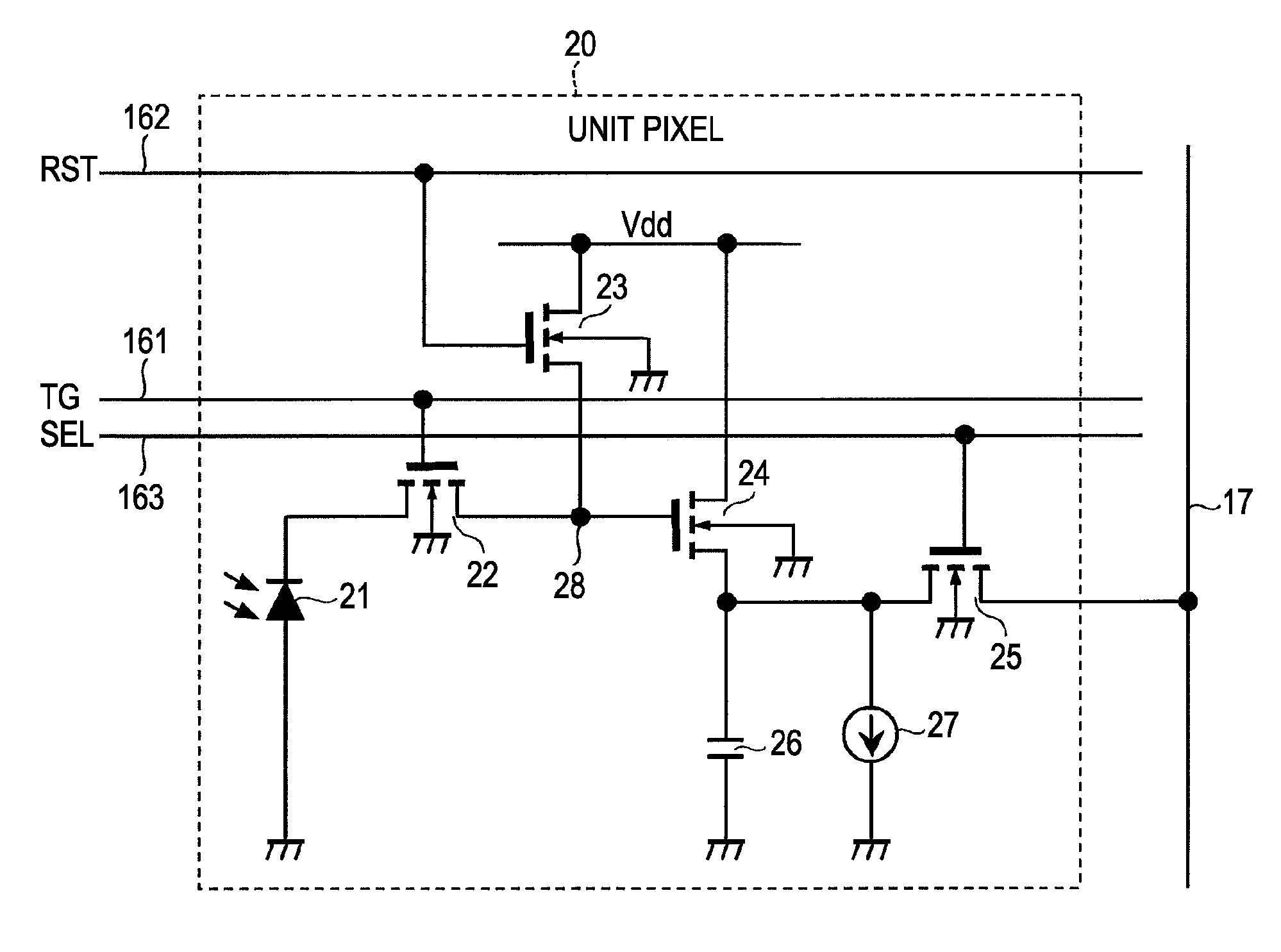
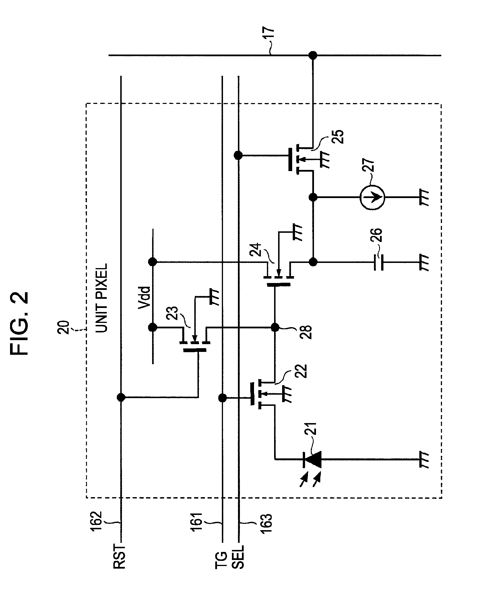
[0048]FIG. 2 is a circuit diagram showing a circuit configuration of a pixel 20 according to a first embodiment of the present invention. As shown in FIG. 2, the pixel 20 according to the first embodiment includes, for example, four transistors 22 to 25, one capacitor 26, and one current source 27 as well as a photodiode 21 that is a photoelectric conversion section, where the capacitor 26 is used as a charge storage capacitor to realize a global shutter function.

[0049]Here, it will be assumed that the four transistors 22 to 25 are N-channel MOS transistors. However, this conductivity type combination of the transistors 22 to 25 is only an explanatory example, and it goes without saying that this part of the pixel 20 is not limited to this combination.

[0050]In this pixel 20, a pixel driving line 16 is composed of, for example, a transfer line 161, a reset line 162, and a selection line 163, and these three lines are connected in common ...

second embodiment

3. the Present Invention

[0092]In the first embodiment of the present invention, each pixel 20 includes its own charge storage capacitor 26 and the like. On the other hand, in the second embodiment of the present invention, some of the components of the pixel 20 are shared by plural pixels, and at least a charge storage capacitor 26 is shared by plural pixels. In this embodiment, the case where some of the components are shared between two adjacent pixels belonging to the same pixel column will be taken as an example.

[Circuit Configuration]

[0093]FIG. 7 is a circuit diagram showing a circuit configuration of pixels 20 with common components according to the second embodiment of the present invention. Components shown in FIG. 7 that are the same as those shown in FIG. 2 have the same reference symbols as those shown in FIG. 2.

[0094]In FIG. 7, it will be assumed that components shared by two pixels 20A-1 and 20A-2 are a reset transistor 23, a amplifying transistor 24, a selection transi...


PUM


Abstract

A solid-state imaging device according to an embodiment of the present invention includes plural pixels, in which each pixel includes: a transfer transistor that transfers electric charge from a photoelectric conversion section to a floating diffusion section; a reset transistor that resets the floating diffusion section; a amplifying transistor that outputs a signal based on the electric charge held by the floating diffusion section; a selection transistor that is provided at the output side of the amplifying transistor and selects a pixel; and a charge storage capacitor that is provided between the amplifying transistor and the selection transistor and stores the quantity of electric charge on the basis the quantity of the electric charge held by the floating diffusion section through the charge-discharge behavior of electric charge through a current source.

Description

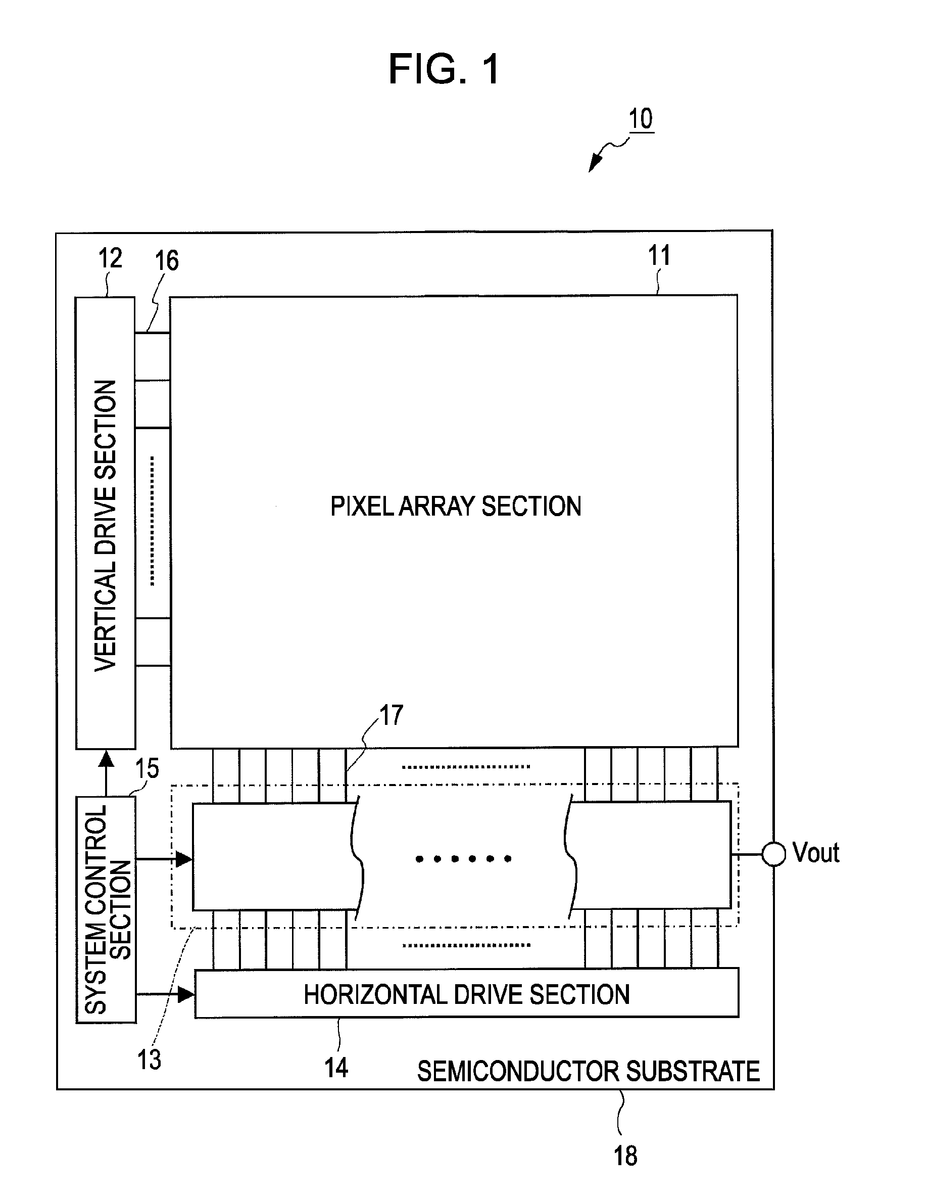
BACKGROUND OF THE INVENTION[0001]1. Field of the Invention[0002]The present invention relates to solid-state imaging devices, driving methods thereof, and electronic apparatuses, and more particularly relates to an X-Y address type solid-state imaging device having a global shutter function, a drive method thereof, and an electronic apparatus including the solid-state imaging device.[0003]2. Description of the Related Art[0004]Solid-state imaging devices are broadly categorized into two types, that is, an X-Y address type solid-state imaging device as represented by a CMOS (complementary metal oxide semiconductor) image sensor, and a charge-transfer type solid-state imaging device as represented by a CCD (charge coupled device) image sensor. Compared with the CCD image sensor, the CMOS image sensor has an advantage in that it can randomly access pixel signals, read out the pixel signals at higher speed, and consumes less electric power.[0005]In many CMOS image sensors, electric char...

Claims


Application Information

Patent Timeline
Patent Type & Authority Patents(United States)
IPC IPC(8): H04N5/335H04N3/14H04N5/369H04N5/372H04N5/353H04N5/3745H04N5/374H01L27/146H04N25/00
CPCH04N5/37452H04N3/155H04N5/353H04N25/771H04N25/778H04N25/532H04N25/77H04N25/53
Inventor WATANABE, KAZUFUMI
Owner SONY CORP
Learn More