Repair method for optical elements having a coating and corresponding optical elements

a technology of optical elements and coatings, applied in the field of optical elements having coatings and corresponding optical elements, can solve the problems of no longer being able to maintain or achieve desired shape, and achieve the effect of simple and effective high-quality repair

Active Publication Date: 2014-08-05
CARL ZEISS SMT GMBH
View PDF8 Cites 0 Cited by
  • Summary
  • Abstract
  • Description
  • Claims
  • Application Information

AI Technical Summary

Benefits of technology

[0006]It is therefore an object of the present invention to provide for the repair of an optical element having a coating in an effective way without, as in the prior art, causing damage to the optical element after the coating is removed and making it unusable. Overall, a repair method and correspondingly adapted or repaired optical elements are intended to be provided, which allow simple and effective but also high-quality repair of optical elements having coatings.
[0007]One aspect of the invention is based on the discovery that with pure cleaving of a damaged coating, the surface quality of the underlying substrate or optical element will not normally be sufficient. Correspondingly, it is necessary to carry out surface processing. The difficulty here, however, is that the desired shape will sometimes no longer be maintained or achievable in the event of extensive surface processing of the optical element. According to this aspect of the invention, therefore, a polishing layer is provided which can be processed very well and therefore allows high geometrical accuracy and low surface roughness of the optical surface of the optical element.
[0008]The polishing layer may be configured in such a way that the polishing layer is easier to polish than the substrate material, so that high geometrical accuracy and low surface roughness can be achieved more easily, or can be achieved for the first time.

Problems solved by technology

The difficulty here, however, is that the desired shape will sometimes no longer be maintained or achievable in the event of extensive surface processing of the optical element.

Method used


Image

  • Repair method for optical elements having a coating and corresponding optical elements
  • Repair method for optical elements having a coating and corresponding optical elements
  • Repair method for optical elements having a coating and corresponding optical elements

Examples


Embodiment Construction

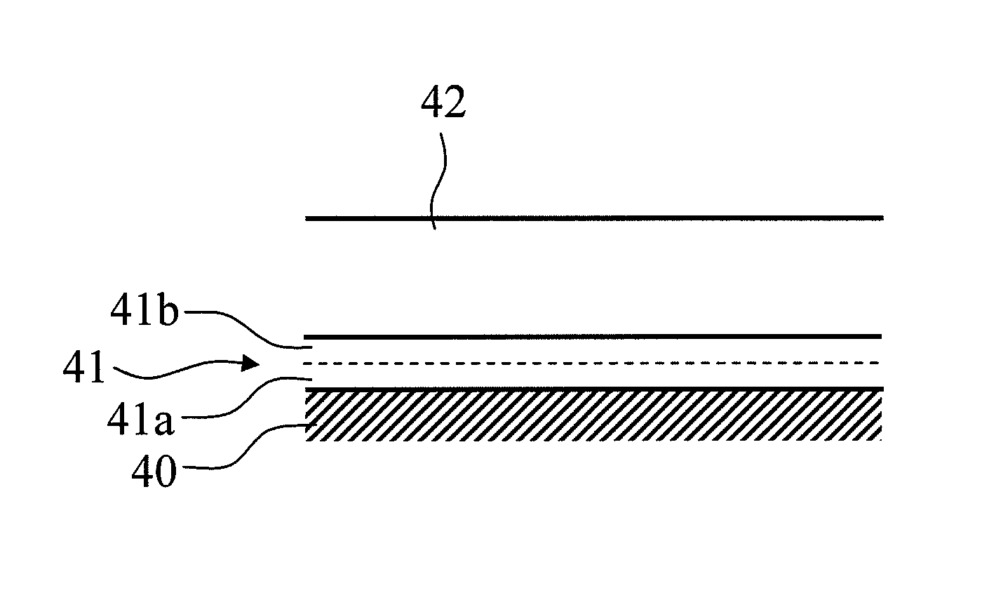
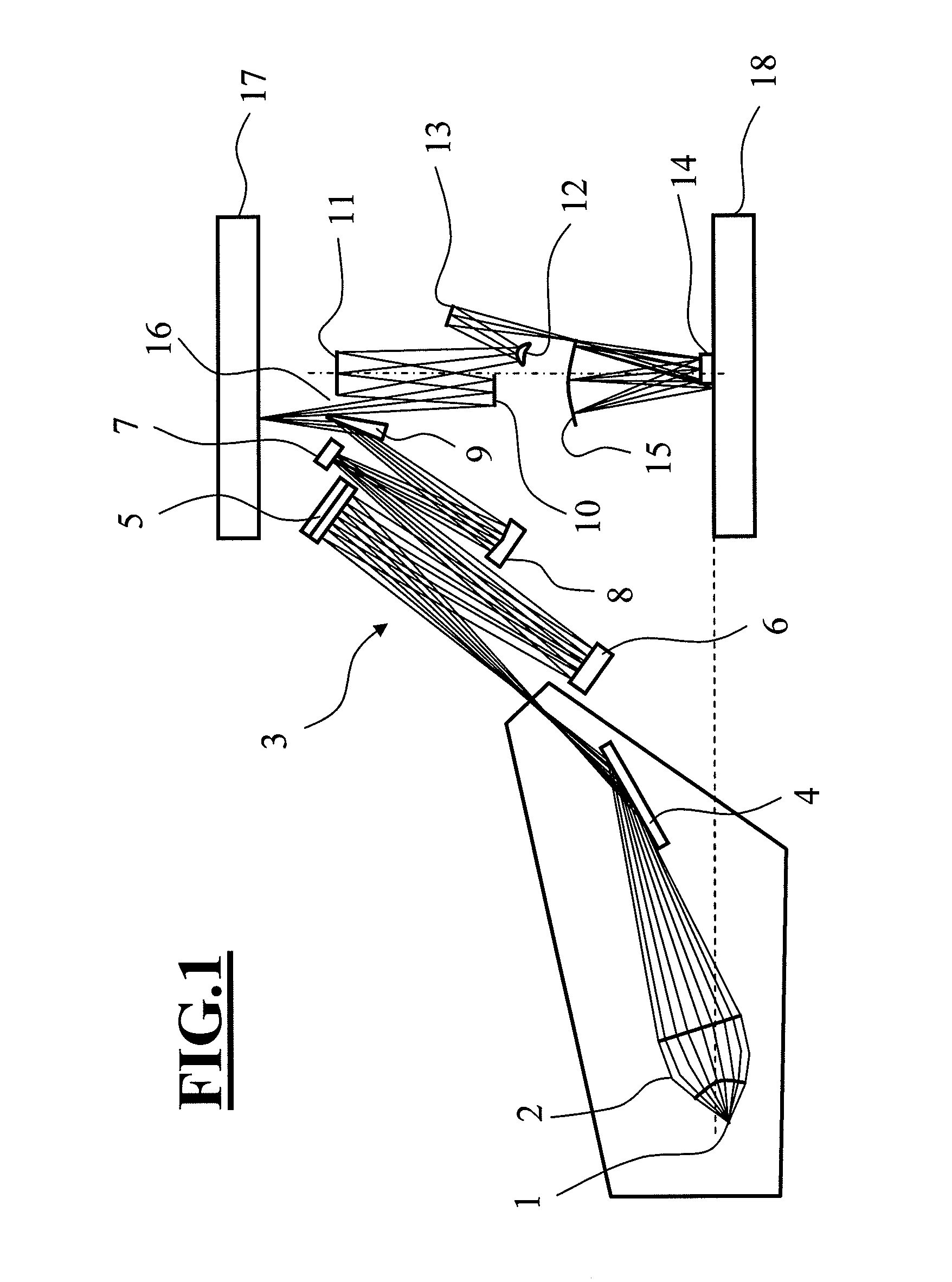
[0037]FIG. 1 shows an EUV projection exposure apparatus in a purely schematic representation, as is described for example in WO 2003 / 014833 A. Such a projection exposure apparatus has an EUV light source 1 and a collector 2 for collecting and forwarding the EUV light. The illumination system 3 comprises a plurality of mirrors 4 to 9 that deflect light rays 16 onto the reticle 17, which has a structure to be imaged onto the wafer 18. The imaging is carried out using projection optics, which in turn have a plurality of mirrors 10 to 15. Although the present invention may be used to repair optical elements having a coating on optical elements in general, i.e. also on refractive optical elements such as lenses, use for reflective optical elements such as mirrors 4 to 15 or collectors 2, which are employed in EUV lithography, is advantageous. The mirrors 4 to 15, like the collector 2, have reflection coatings which may be constructed from a multiplicity of thin layers in order to form a ...


PUM

PropertyMeasurementUnit
wavelengthsaaaaaaaaaa
thicknessaaaaaaaaaa
thicknessaaaaaaaaaa

Abstract

A method for repairing optical elements having a coating, in which the coating is fully or partially removed or left on the optical element, a polishing layer being provided in the coating or a polishing layer being applied, which allows simple processing of the surface to achieve high geometrical accuracy and lower surface roughness. A new coating is applied onto the corresponding polishing layer. Also addressed are corresponding optical elements, including optical elements recycled according to the method.

Description

[0001]This application claims benefit of U.S. Provisional Application No. 61 / 019,763, filed Jan. 8, 2008, which is incorporated into this application by reference.FIELD AND BACKGROUND OF THE INVENTION[0002]The present invention relates to a method for repairing optical elements having a coating, as well as to optical elements correspondingly prepared therefor and to optical elements repaired by the corresponding method.[0003]For the production of microelectronic components or other micro- or nanostructured elements, lithography methods are used in which light, i.e. electromagnetic radiation in general, with short wavelengths is being used increasingly in order to be able to achieve a corresponding resolution. For example, EUV (extreme ultraviolet) light with wavelengths in the range of 13 nm may be used as electromagnetic radiation. The corresponding projection exposure apparatus have optics which comprise a multiplicity of mirrors. Furthermore a collector, which collects the light ...

Claims


Application Information

Patent Timeline
Patent Type & Authority Patents(United States)
IPC IPC(8): B05D3/14G02B1/10B05D3/06B32B17/00G02B1/02B05D3/00B05D5/06
CPCG02B1/12G02B1/02G02B5/0891Y10T428/31678Y10T428/30Y10T428/265Y10T428/31504G02B1/10Y10T428/263
Inventor BOEHM, THURE
Owner CARL ZEISS SMT GMBH
Why Eureka
Try Eureka