

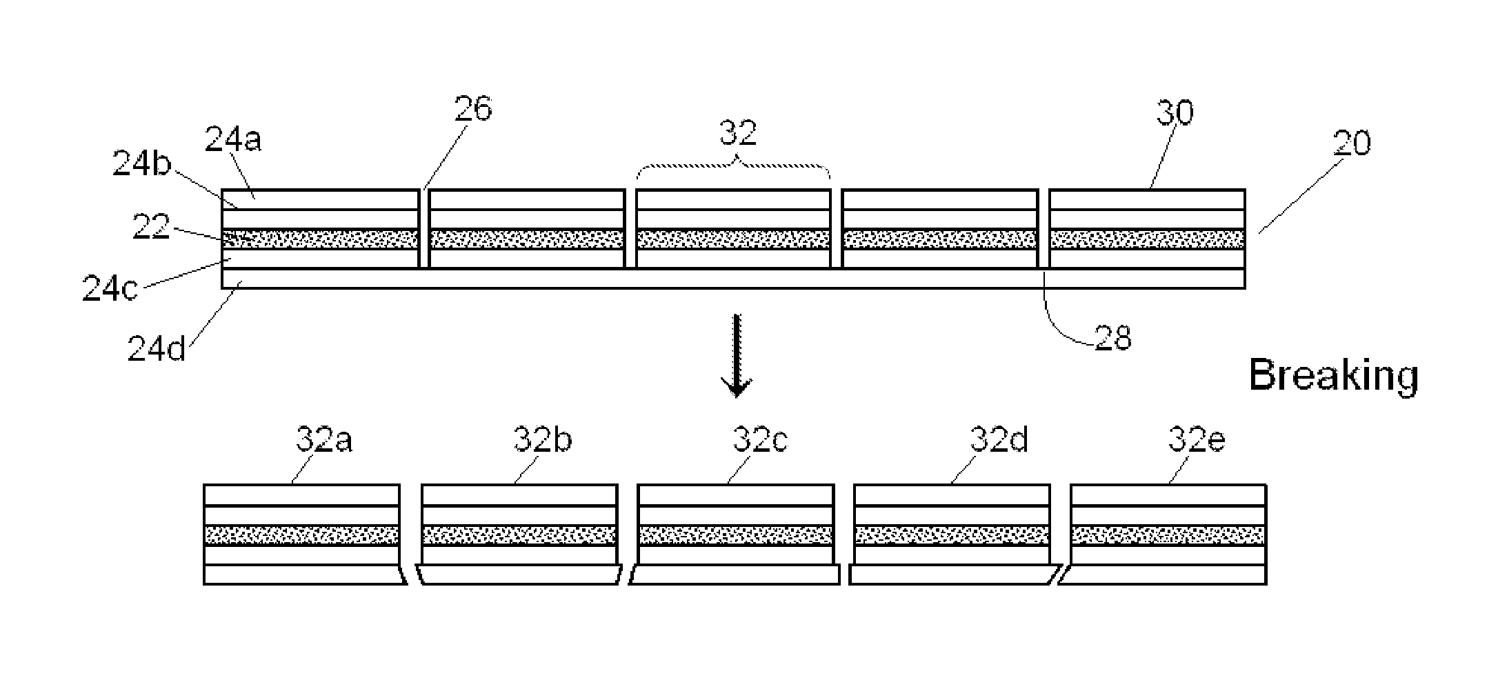
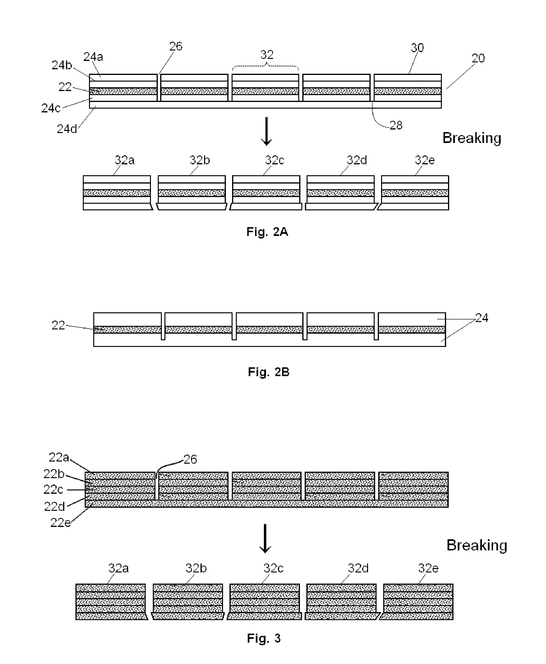
Light emissive ceramic laminate and method of making same
a technology of light emissive ceramics and laminates, which is applied in the manufacture of electrode systems, cold cathode manufacturing, electric discharge tubes/lamps, etc., can solve the problems of weak light scattering, loss of white light emission, poor resultant luminosity generated by these luminescent layers, etc., and achieve the effect of eliminating the expensive dicing process
- Summary
- Abstract
- Description
- Claims
- Application Information
AI Technical Summary
Benefits of technology
Problems solved by technology
Method used
Image

Examples
examples
IQE Measurement and Comparison of Powders
[0049]The present invention will be explained in detail with reference to Examples which are not intended to limit the present invention.
[0050]1. Green Sheet Preparation for Non-Emissive (YAG) Layers for Laminated Composite
[0051]A 50 ml high purity Al2O3 ball mill jar was filled with 55 g of Y2O3-stabilized ZrO2 ball of 3 mm diameter. Then, in a 20 ml glass vial, 0.153 g dispersant (Flowlen G-700. Kyoeisha), 2 ml xylene (Fisher Scientific, Laboratory grade) and 2 ml ethanol (Fisher Scientific, reagent alcohol) were mixed until the dispersant was dissolved completely. The dispersant solution and tetraethoxysilane, as sintering aid (0.038 g, Fluka), were added to a ball mill jar.
[0052]Y2O3 powder (3.984 g, 99.99%, lot N-YT4CP, Nippon Yttrium Company Ltd.) with a BET surface area of 4.6 m2 / g and Al2O3 powder (2.998 g, 99.99%, grade AKP-30, Sumitomo Chemicals Company Ltd.) with a BET surface area of 6.6 m2 / g were added to ball mill jar. The total...
PUM
| Property | Measurement | Unit |
|---|---|---|
| thickness | aaaaa | aaaaa |
| particle size | aaaaa | aaaaa |
| size | aaaaa | aaaaa |
Abstract
Description
Claims
Application Information