Optoelectronic device containing at least one active device layer having a wurtzite crystal structure, and methods of making same

a technology of optoelectronic devices and active devices, which is applied in the direction of semiconductor laser structure details, lasers, semiconductor lasers, etc., can solve the problems of preventing the realization of white light by color mixing, frequency doubling, and sorely lagging performance of electroluminescent green light-emitting diodes

Inactive Publication Date: 2014-10-14
VERLASE TECH
View PDF2 Cites 63 Cited by
  • Summary
  • Abstract
  • Description
  • Claims
  • Application Information

AI Technical Summary

Problems solved by technology

However, performance of electroluminescent green-light-emitting diodes has been sorely lagging, preventing the realization of white light by color mixing, such as by trichromatic LEDs.
Examples of such techniques and their drawbacks include: a) frequency doubling (low efficiency); b) using InGaN by modifying crystal orientation of a starting GaN substrate (temperature instability, limited solubility of indium in GaN, high-cost substrate platform, and increased dislocation densities with increased indium content); c) using II-VI wide-band-gap semiconductor materials (short continuous operation limits due to crystal defects); d) using GaInP alloy coatings on GaAs substrate (green LEDs only, no green LDs); e) using NZnO coatings on p-type GaN substrates (broadband green LEDs and no LDs); and f) using quantum dots in lieu of quantum wells (green LEDs only, no green LDs).

Method used


Image

  • Optoelectronic device containing at least one active device layer having a wurtzite crystal structure, and methods of making same
  • Optoelectronic device containing at least one active device layer having a wurtzite crystal structure, and methods of making same
  • Optoelectronic device containing at least one active device layer having a wurtzite crystal structure, and methods of making same

Examples


Embodiment Construction

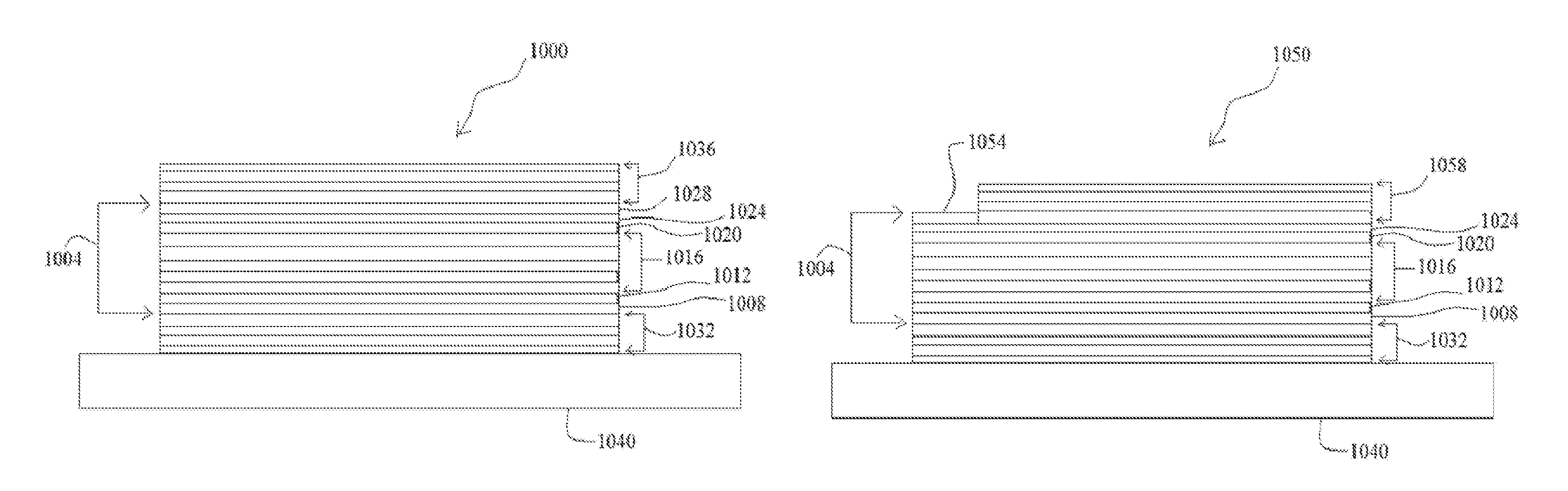
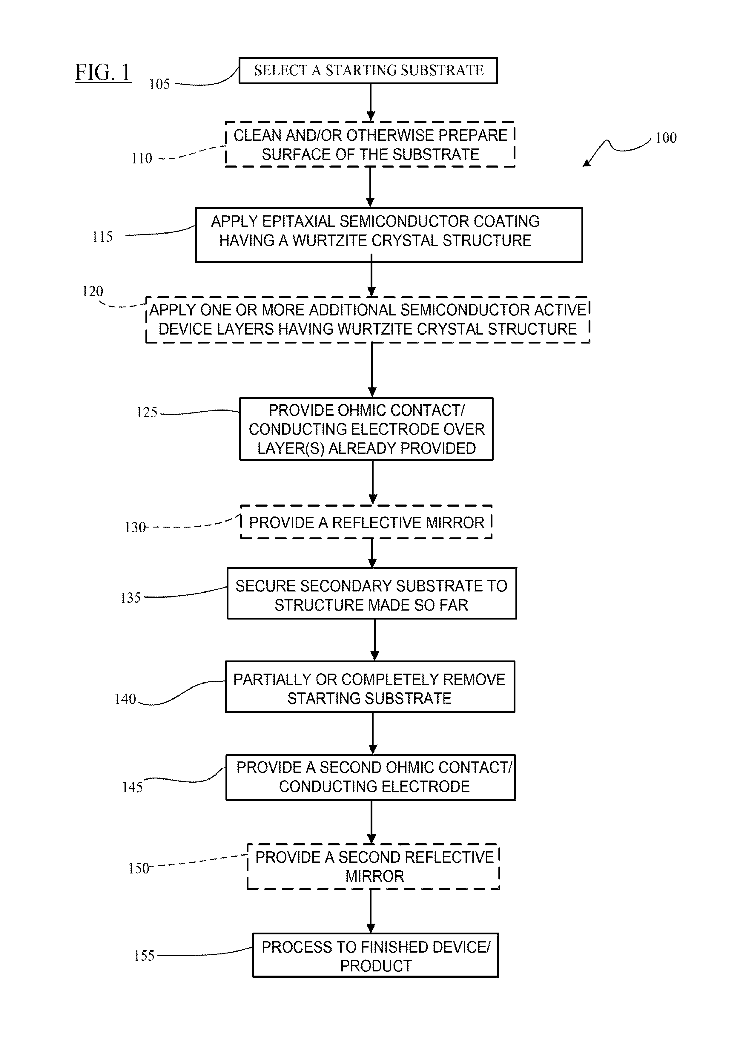
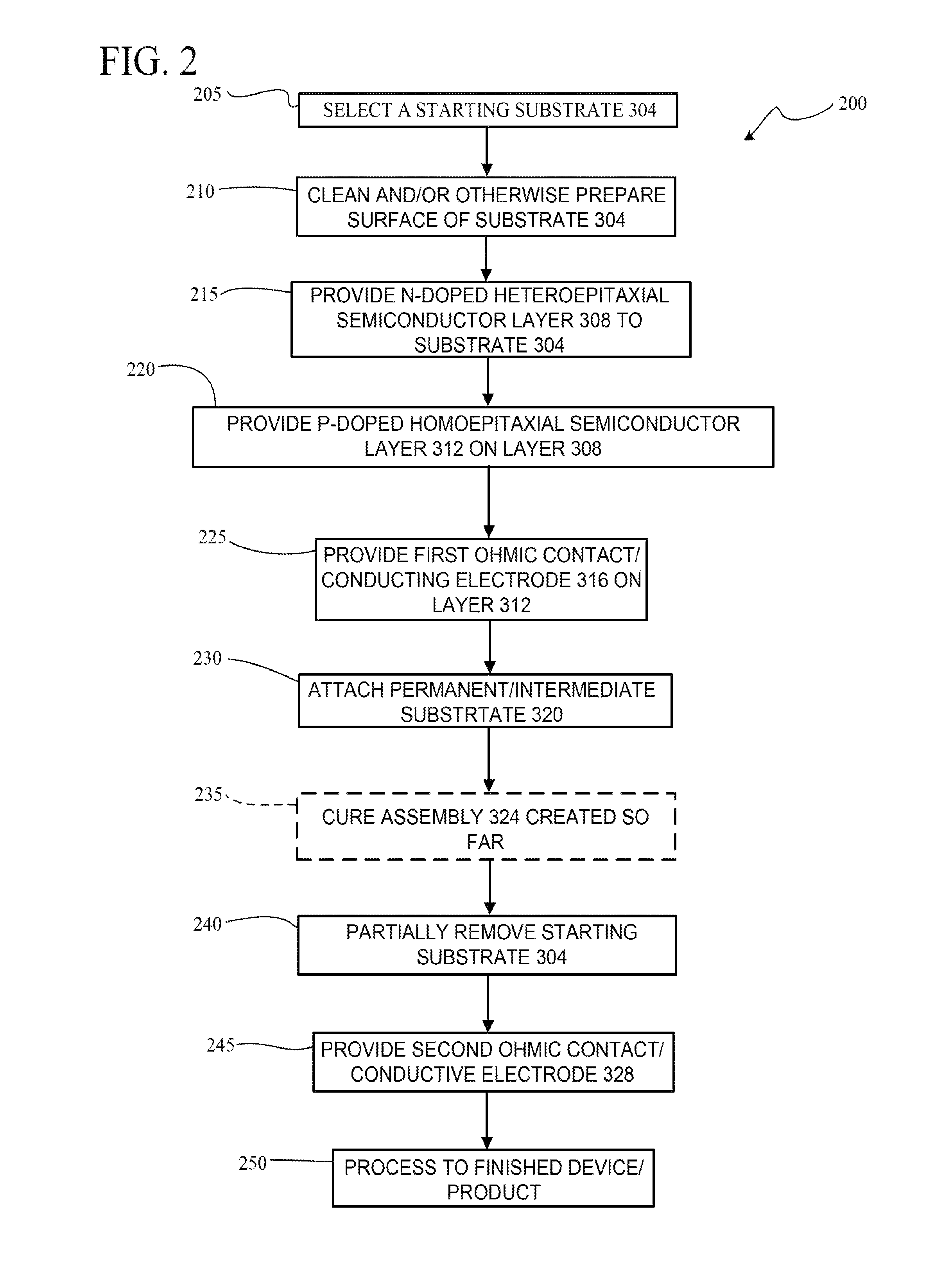
[0022]Referring now to the drawings, FIG. 1 illustrates a generalized method 100 of fabricating an optoelectronic device, for example, a light-emitting diode (LED), laser diode (LD), etc., that includes one or more epitaxial layers that each have a wurtzite crystal structure. Depending on the materials and processes utilized at the various steps of method 100, the method can produce high-power, high-performance, and long lasting optoelectronic devices, including true green LEDs and LDs, at a low cost. Such devices can have significant ramifications for a variety of applications, including solid state lighting, projection displays (e.g., micro-, nano-, and pico-projectors), information displays, video monitors and televisions, ophthalmic surgery, medical imaging (e.g., DNA sequencing machines, fiber-optic communications, non-lethal threat detection, and visual warning, among many others. An important contributor to the efficacy of method 100 in creating low cost high quality optoelec...


PUM


Abstract

Optoelectronic devices, such as light-emitting diodes, laser diodes, image sensors, optical detectors, etc., made by depositing (growing) one or more epitaxial semiconductor layers on a monocrystalline lamellar / layered substrate so that each layer has a wurtzite crystal structure. In some embodiments, the layers are deposited and then one or more lamellas of the starting substrate are removed from the rest of the substrate. In one subset of such embodiments, the removed lamella(s) is / are partially or entirely removed. In other embodiments, one or more lamellas of the starting substrate are removed prior to depositing the one or more wurtzite-crystal-structure-containing layer(s).

Description

RELATED APPLICATION DATA[0001]This application claims the benefit of priority of U.S. Provisional Patent Application Ser. No. 61 / 516,602, filed on Apr. 6, 2011, and titled “Novel Method of Making a Laser Diode,” and U.S. Provisional Patent Application Ser. No. 61 / 573,709, filed on Sep. 12, 2011, and titled “Novel Method of Making a Laser Diode,” each of which is incorporated by reference herein in its entirety.FIELD OF THE INVENTION[0002]The present invention generally relates to the field of semiconductor-based optoelectronic devices. In particular, the present invention is directed to an optoelectronic device containing at least one active device layer having a wurtzite crystal structure, and methods of making same.BACKGROUND[0003]As is well known, the human eye is sensitive to electromagnetic radiation having a wavelength in a range from about 400 nm to about 700 nm, i.e., in the visible spectrum. Of this range of sensitivity, the human eye is most sensitive to radiation at about...

Claims


Application Information

Patent Timeline
Patent Type & Authority Patents(United States)
IPC IPC(8): H01L21/28H01L21/02H01L33/00H01L33/26H01S5/02H01S5/042H01S5/183H01S5/327H01S5/347
CPCH01L31/035236B82Y20/00H01L33/005H01S5/0206H01S5/0425H01L31/032H01L33/0087H01L21/02568H01L31/0324H01L31/036H01S5/125H01S5/183H01L33/26H01L21/02521H01L33/18H01L21/0237H01L31/0296H01S5/347H01S5/327H01L21/02417H01S5/187H01L21/024H01L21/02551H01L33/46H01L33/0079H01L21/02557H01L31/02325H01L33/06H01S5/0217H01L33/0083H01L33/28H01L33/0093H01L33/32
Inventor JAIN, AJAYKUMAR, R.
Owner VERLASE TECH
Why Eureka
Try Eureka