Mixed-phase nitride film field emission cathode with enhanced electron emission and preparation method thereof

A Field Emission Cathode, Electron Emission Technology

Active Publication Date: 2011-12-14
BEIJING UNIV OF TECH
View PDF3 Cites 2 Cited by
  • Summary
  • Abstract
  • Description
  • Claims
  • Application Information

AI Technical Summary

Problems solved by technology

[0005] The purpose of the present invention is to overcome the unavoidable defects of existing field emission cathodes such as poor emission stability, high open electric field, low emission current density, complicated preparation process, and high production cost, and provide a wurtzite hexagonal phase and sphalerite cubic Field emission cathode suitable for vacuum microelectronic devices with a mixed-phase nano-film structure, low threshold electric field, high emission current density, simple process, and long service life and its preparation method

Method used


Image

  • Mixed-phase nitride film field emission cathode with enhanced electron emission and preparation method thereof
  • Mixed-phase nitride film field emission cathode with enhanced electron emission and preparation method thereof
  • Mixed-phase nitride film field emission cathode with enhanced electron emission and preparation method thereof

Examples


Embodiment 1

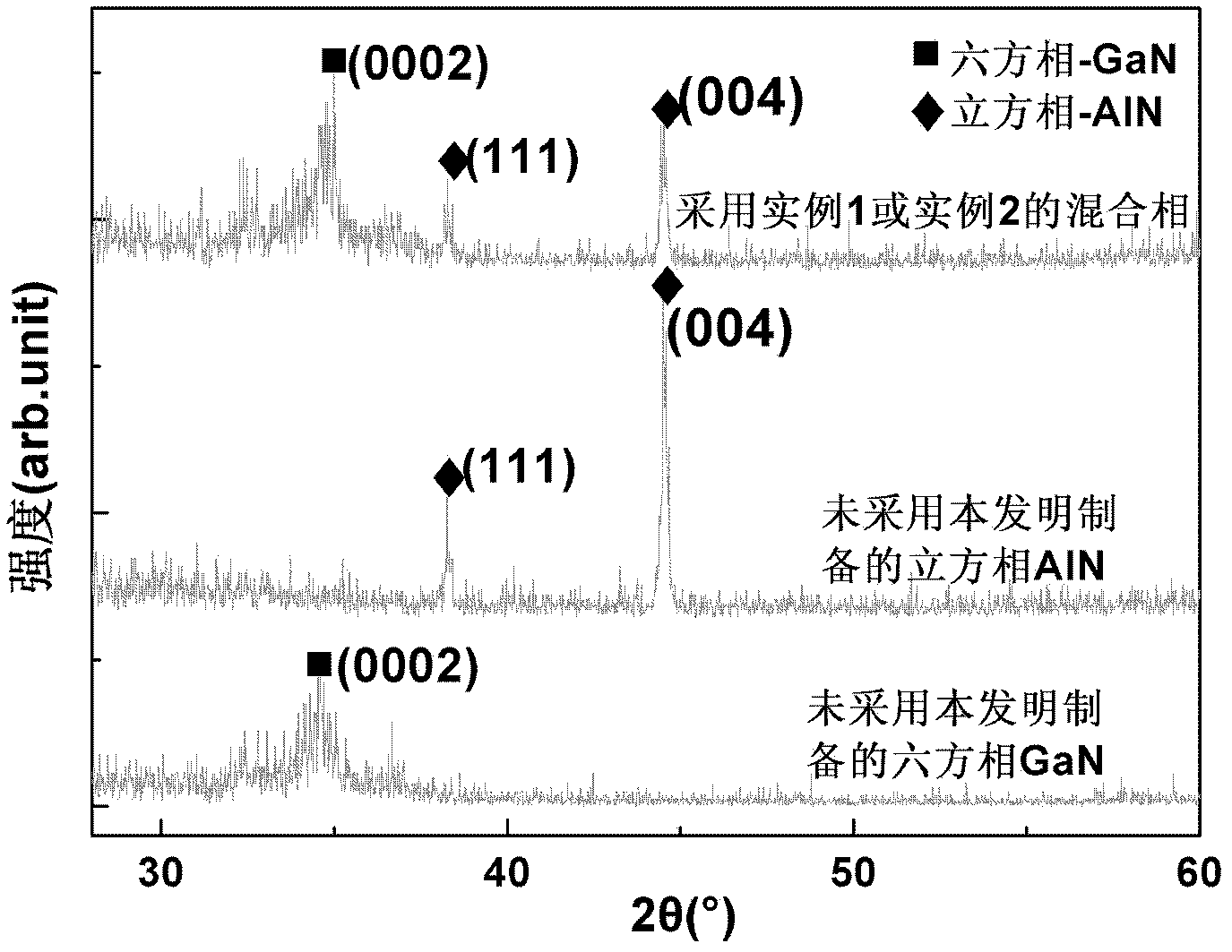
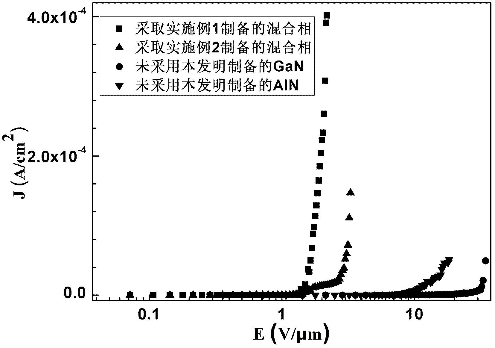
[0025] The target material in this embodiment is uniformly mixed powder of AlN and GaN (purity>98%, molar ratio 1:1) which is sintered into a target. Use polished n-type (100) doped silicon as the substrate, soak the substrate in 5% HF acid for 3 minutes, then clean it with deionized water, dry the surface of the substrate, and put the substrate into the laser pulse deposition system chamber, pump the deposition chamber to approximately 7 x 10 -4 Pa, and heat the substrate to 900°C. The growth conditions are: supply nitrogen with a purity of 99.99% as a protective gas and adjust the working pressure of the deposition chamber to 1Pa, the distance between the target and the base to 80mm, set the frequency of the pulsed laser to 13Hz, the pulse energy to 350mJ / pulse, and the deposition time to be 300s , deposit a 150nm thick layer of unintentionally doped n-type Al 0.5 Ga 0.5 The N thin film was annealed in situ for 30 min, and finally dropped to room temperature under the pro...

Embodiment 2

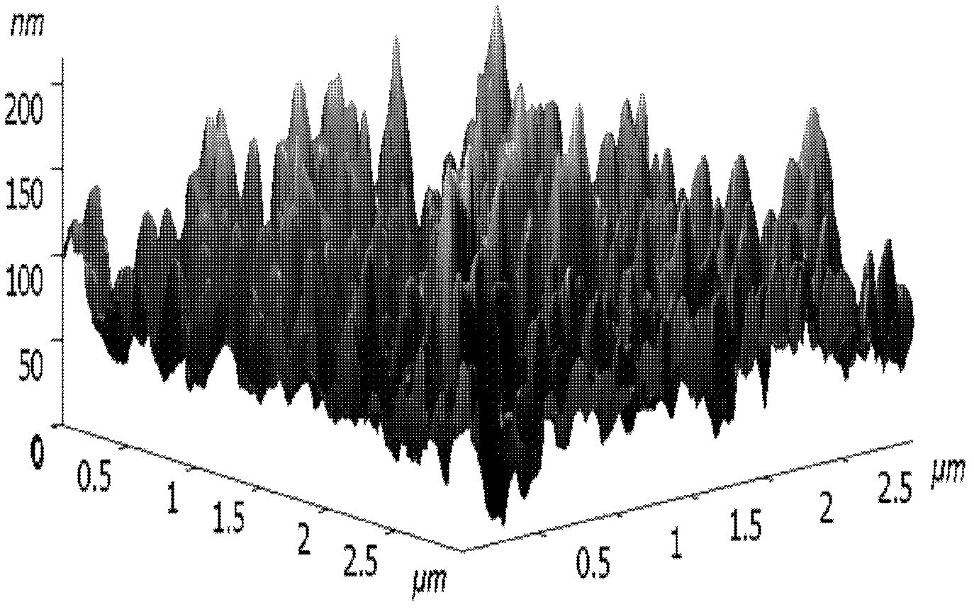
[0027] The target material in this embodiment is uniformly mixed powder of AlN and GaN (purity>98%, molar ratio 1:1) which is sintered into a target. Use polished n-type (111) doped silicon as the substrate, soak the substrate in 7% HF acid for 3 minutes, then clean it with deionized water, dry the surface of the substrate, and put the substrate into the laser pulse deposition system chamber, pump the deposition chamber to approximately 7 x 10 -4 Pa, and heat the substrate to 850°C. The growth conditions are as follows: supply nitrogen with a purity of 99.99% as a protective gas and adjust the working pressure of the deposition chamber to 1Pa, the target base distance to 60mm, set the pulse laser frequency to 13Hz, pulse energy to 375mJ / pulse, and deposit a layer of 280nm Thick unintentionally doped n-type Al 0.5 Ga 0.5 The N thin film was annealed in situ for 30 min, and finally dropped to room temperature under the protection of nitrogen. The nano-film has a surface root...

Embodiment 3

[0029] The target material in this embodiment is uniformly mixed powder of AlN and GaN (purity>98%, molar ratio 1:1) which is sintered into a target. Use polished Al as the substrate, put the substrate into the cavity of the laser pulse deposition system, and pump the deposition chamber to about 2×10 -3 Pa, and heat the substrate to 650°C. The growth conditions are as follows: supply nitrogen with a purity of 99.99% as a protective gas and adjust the working pressure of the deposition chamber to 5Pa, the target base distance to 60mm, set the pulse laser frequency to 13Hz, pulse energy to 400mJ / pulse, and deposit a layer of 150nm Thick unintentionally doped n-type Al 0.5 Ga 0.5 The N thin film was annealed in situ for 30 min, and finally dropped to room temperature under the protection of nitrogen.


PUM

PropertyMeasurementUnit
thicknessaaaaaaaaaa
surface roughnessaaaaaaaaaa

Abstract

The invention relates to a field emission cathode with an electron emission-enhanced mixed phase nitride film and a preparation method for the field emission cathode, and belongs to the technical field of field emission cathodes. The cathode is made of a mixture of GaN and AlN, has a hexagonal wurtzite crystal structure and a cubic sphalerite crystal structure, and comprises the component of AlxGa1-xN, wherein x is more than 0 and is less than or equal to 0.95. The preparation method comprises the following steps of: putting a substrate and a target material formed by sintering the GaN and the AlN into a laser pulse deposit system, vacuumizing, heating the substrate, introducing protective gas, and preparing a nanometer film with an aluminum gallium nitride wurtzite hexagonal phase and a sphalerite cubic phase which coexist by using the laser pulse deposit system. Compared with a single-phase film, the nanometer film has the advantage that: the field emission cut-in voltage and the maximum current density are improved by 2 to 5 orders of magnitude. By the nanometer film with the two phases which coexist, the improvement on the field emission performance of the film and the commercialization of a field emission display is facilitated, so the field emission cathode has an obvious application prospect and a potential economic benefit.

Description

technical field [0001] The invention belongs to the technical field of field emission cathodes, in particular to a semiconductor nano-film with a metastable mixed phase, which is applied to high-resolution field emission displays, microwave amplifiers, electron beam induced light sources, etc., and is especially suitable for field emission flat panel displays of the cathode. Background technique [0002] The core component of the field emission display is the field emission cold cathode. Field emission cathode is the core technology of vacuum microelectronic devices, and it is also the main research object of vacuum microelectronics. As one of the most potential applications of field emission technology, field emission flat panel display (FED) has become a project that various countries are competing to develop. According to the market report of DisplaySearch, in 2010, the revenue of the global flat panel display field reached 110 billion US dollars, accounting for 94% of ...

Claims


Application Information

Patent Timeline
Patent Type & Authority Applications(China)
IPC IPC(8): H01J1/308H01J29/04H01J9/02
Inventor 王如志宋志伟赵维严辉王波张铭宋雪梅朱满康侯育冬刘晶冰汪浩
Owner BEIJING UNIV OF TECH
Why Eureka
Try Eureka