Nitride semiconductor epitaxial wafer and field effect nitride transistor

a technology of nitride semiconductor and epitaxial wafer, which is applied in the direction of semiconductor devices, electrical equipment, basic electric elements, etc., can solve problems such as current collapse, and achieve the effect of suppressing current collaps

Active Publication Date: 2017-10-03
SUMITOMO CHEM CO LTD
View PDF19 Cites 1 Cited by
  • Summary
  • Abstract
  • Description
  • Claims
  • Application Information

AI Technical Summary

Benefits of technology

[0018]Accordingly, it is an object of the present invention to provide a nitride semiconductor epitaxial wafer and a field effect nitride transistor, capable of suppressing current collapse.
[0037]According to the present invention, it is possible to provide the nitride semiconductor epitaxial wafer and the field effect nitride transistor that are able to suppress the current collapse.

Problems solved by technology

In field effect nitride transistors, there arises the problem of current collapse.

Method used


Image

  • Nitride semiconductor epitaxial wafer and field effect nitride transistor
  • Nitride semiconductor epitaxial wafer and field effect nitride transistor
  • Nitride semiconductor epitaxial wafer and field effect nitride transistor

Examples


embodiment

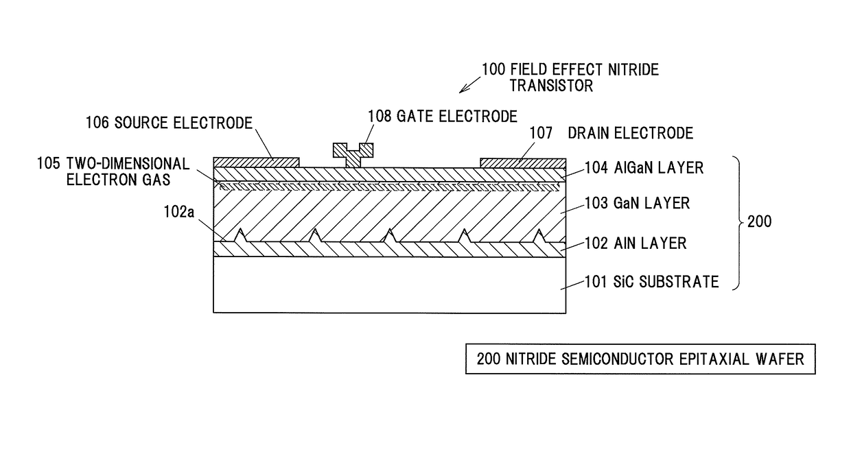
[0045]FIG. 1 is a cross-sectional view showing a schematic configuration example of a field effect nitride transistor 100 in an embodiment according to the invention.

[0046]This field effect nitride transistor 100 is a GaN based HEMT (High Electron Mobility Transistor), and includes, e.g., a silicon carbide (SiC) substrate 101 as a substrate. Over the SiC substrate 101, there are epitaxially grown an aluminum nitride (AlN) layer 102, a gallium nitride (GaN) layer 103, and an aluminum gallium nitride (AlGaN) layer 104 in this order to form a nitride semiconductor epitaxial wafer 200, and a source electrode 106, a drain electrode 107 and a gate electrode 108 are formed on the AlGaN layer 104.

[0047]As the SiC substrate 101, a polytype 4H or polytype 6H semi-insulative SiC substrate may be used. Here, the number in 4H or 6H denotes a repetition period in a c-axis orientation, and H therein denotes a hexagonal crystal. As the substrate, in order to reduce parasitic capacitance and provide...

example 1

[0062]First, as a substrate, a polytype 4H or polytype 6H semi-insulative SiC substrate 101 is prepared. The SiC substrate 101 is then introduced into an MOVPE (Metal Organic Vapor Phase Epitaxy) apparatus, to be heat treated for 5 minutes at a set temperature of 1175 degrees Celsius in H2 / N2 gas mixture flow atmosphere that does not contain NH3. This heating cleans the surface of the SiC substrate 101.

[0063]Next, an ammonia gas (H2 / NH3 gas mixture) is introduced into a reactor of the MOVPE apparatus for 25 seconds at the temperature held at 1175 degrees Celsius. This ammonia gas flow prevents desorption of nitrogen atoms in the subsequent AlN forming step, to make AlN high quality.

[0064]Then, an AlN layer 102 with a film thickness of 12 nm is formed at the temperature held at 1175 degrees Celsius by using an ammonia gas and a trimethyl aluminum (TMA) as raw materials.

[0065]Then, a H2 / NH3 gas mixture is fed into the reactor of the MOVPE apparatus such that the H2 / NH3 ratio is 3, to ...

examples 2 to 5

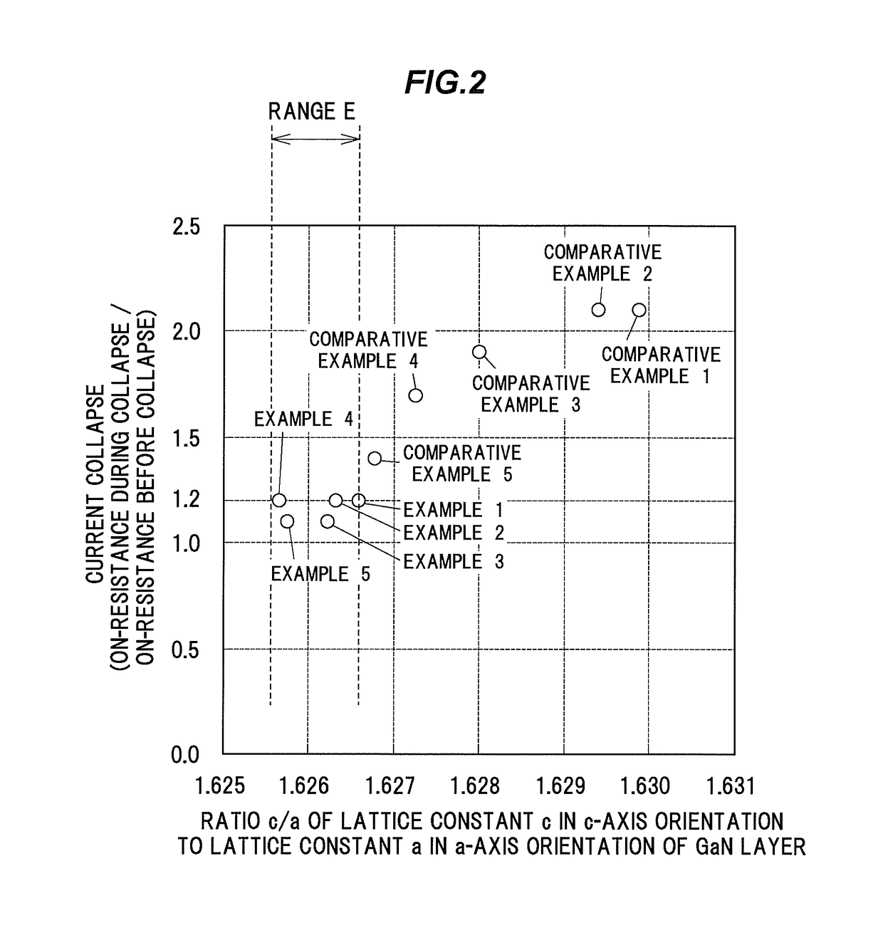
[0071]In Examples 2 to 5, a field effect nitride transistor was produced in the same manner as in Example 1, except that the H2 / NH3 ratio in the H2 / NH3 gas mixture during the SiC substrate cooling step after the formation of the AlN layer was altered within a range not greater than 4 (i.e. ≦4). The H2 / NH3 gas mixture during the SiC substrate cooling step after the formation of the AlN layer was fed by adjusting the H2 / NH3 ratio to 4 in Example 2, to 2.5 in Example 3, to 1 in Example 4, and to 2 in Example 5. The ratios c / a of the lattice constants of the GaN layers formed in Examples 2 to 5 were each 1.6256 to 1.6263. FIG. 2 shows measured results of the current collapse.


PUM


Abstract

A nitride semiconductor epitaxial wafer includes a substrate, a GaN layer provided over the substrate, and an AlGaN layer provided over the GaN layer. The GaN layer has a wurtzite crystal structure, and a ratio c / a of a lattice constant c in a c-axis orientation of the GaN layer to a lattice constant a in an a-axis orientation of the GaN layer is not more than 1.6266.

Description

[0001]The present application is based on Japanese patent application No. 2012-12920 filed on Jan. 25, 2012 and Japanese patent application No. 2012-078469 filed on Mar. 30, 2012, the entire contents of which are incorporated herein by reference.BACKGROUND OF THE INVENTION[0002]1. Field of the Invention[0003]This invention relates to a nitride semiconductor epitaxial wafer and a field effect nitride transistor.[0004]2. Description of the Related Art[0005]In conventional art, nitride semiconductors containing indium (In), gallium (Ga), aluminum (Al), nitrogen (N) and the like have been being developed and put into practical use as materials for innovative high-efficiency light emitting devices which cover most of ultraviolet to visible light regions, by controlling a group III element composition ratio therein.[0006]In addition, the nitride semiconductors have been put into practical use as materials for electronic devices to achieve high efficiencies and high outputs in high frequen...

Claims


Application Information

Patent Timeline
Patent Type & Authority Patents(United States)
IPC IPC(8): H01L29/20H01L21/02H01L29/04H01L29/16H01L29/778
CPCH01L29/2003H01L21/0237H01L21/0254H01L21/0259H01L21/0262H01L21/02378H01L21/02458H01L21/02494H01L21/02502H01L29/04H01L29/1608H01L29/7786
Inventor TANAKA, TAKESHIKANEDA, NAOKINARITA, YOSHINOBU
Owner SUMITOMO CHEM CO LTD
Why Eureka
Try Eureka