Method and apparatus for a clock and signal distribution network for a 60 GHz transmitter system

a technology of clock and signal distribution network, which is applied in the direction of generating/distributing signals, pulse techniques, instruments, etc., can solve the problems of reducing the purity of the desired signal being transferred, and achieve the effect of increasing the number of transmitters, less power, and less area

Active Publication Date: 2014-10-28
TENSORCOM
View PDF23 Cites 1 Cited by
  • Summary
  • Abstract
  • Description
  • Claims
  • Application Information

AI Technical Summary

Benefits of technology

[0012]An embodiment is presented to form the power divider and quadrature hybrid from lumped capacitors and inductors instead of using transmission lines to form these capacitors and inductors. The sinusoidal combiner also uses lumped capacitors and inductors. Transmission lines require more area to emulate the equivalent capacitance and inductance of lumped capacitors and inductors. Using lumped capacitors and inductors reduces the area usage by as much as 80%. In addition, the insertion loss would decrease by the square root of the area used since the resistive loss would be proportional to the length of the traces used to form the transmission lines or lumped elements.
[0015]Another embodiment creates a low power 60 GHz distribution network that can be scaled as the number of transmitters is increased. The composite 60 GHz clock offers the ability to transfer the I and Q clocks over the surface of the die to multiple transmitters, multiple receivers or both multiple transmitters and multiple receivers using less power and less area.
[0017]A further embodiment is to use a supply inductor to couple the drain of the PA transistor to the power supply. The supply inductor does not behave as an RF choke at either the fundamental or second harmonic. Instead, the supply inductor is tuned at the second harmonic with the parasitic capacitance of the drain of the PA transistor. Then, a load capacitance which is located on the output signal pad is adjusted at the fundamental frequency to insure that the current waveform and voltage waveforms at the drain of the PA transistor do not overlap. This feature minimizes the parasitic power dissipation and allows for the energy to be applied to the antenna.
[0018]In another embodiment, the pre-driver stage of the PA is designed as a Class-A stage, maximizing the voltage swing delivered to the gate of the PA switch or transistor. To minimize the inductive coupling between the pre-driver stage and the PA (Power amplifier) stage and in turn ensure PA stability, the resonance network of the driver stage is implemented by a load formed by a CPW line coupled to the supply and an AC coupling capacitor coupling the drain of the pre-driver to the gate of the PA transistor.

Problems solved by technology

However, these circuit components formed on the die would use up valuable real-estate on the semiconductor substrate.
Second harmonics due to the non-linear behavior of the transistor introduces an additional difficulty in power amplifier design. These second harmonics can distort the desired waveform at the antenna and reduce the purity of the desired signal being transferred. Several solutions are presented to remove these second order distortions as well as using them advantageously to improve the quality of the signal being delivered to the antenna.

Method used


Image

  • Method and apparatus for a clock and signal distribution network for a 60 GHz transmitter system
  • Method and apparatus for a clock and signal distribution network for a 60 GHz transmitter system
  • Method and apparatus for a clock and signal distribution network for a 60 GHz transmitter system

Examples


Embodiment Construction

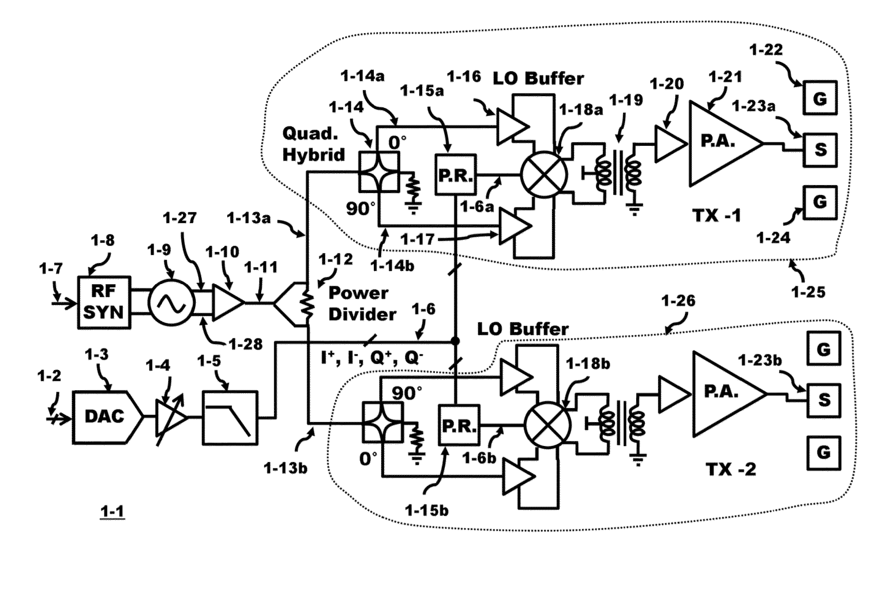
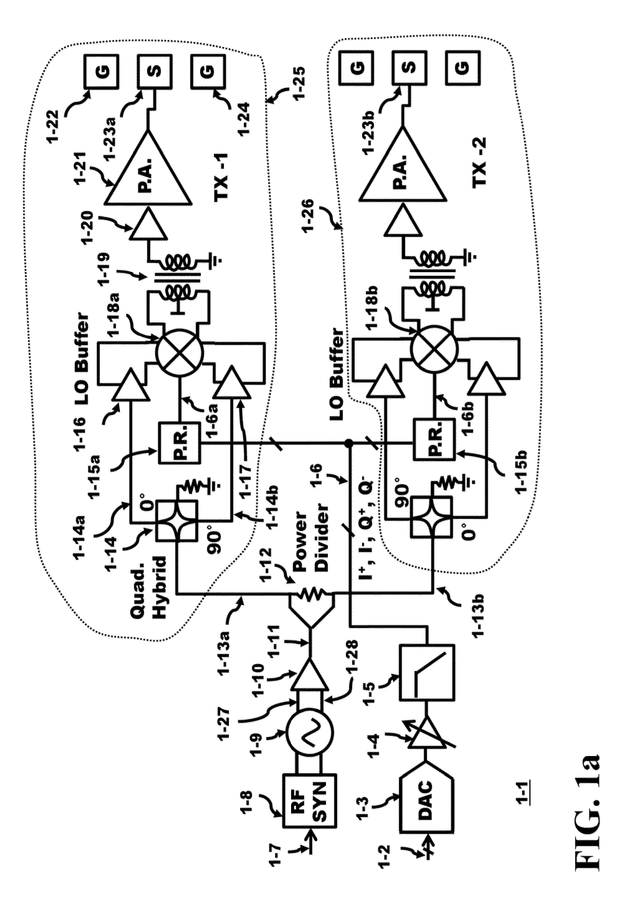
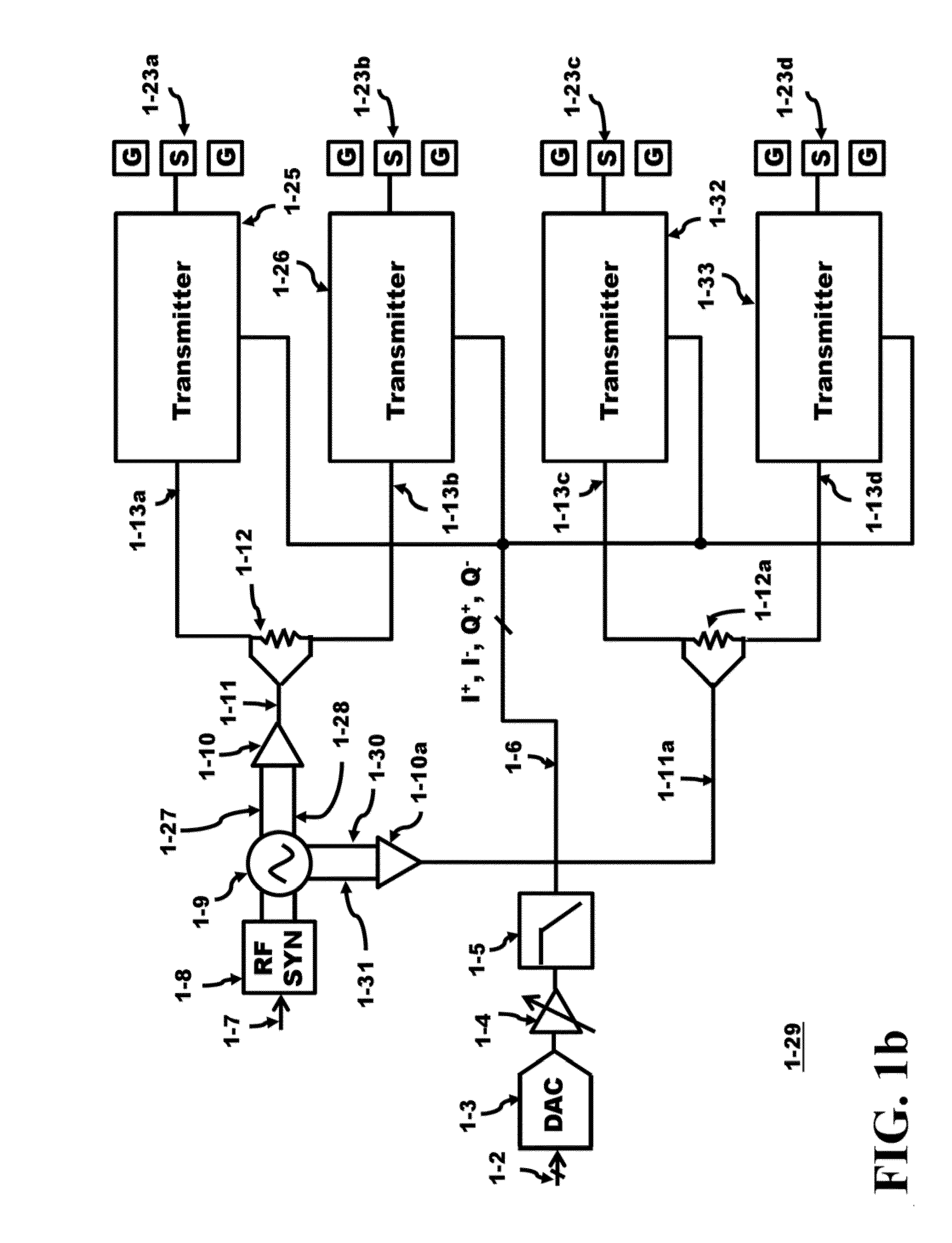
[0034]FIG. 1a illustrates 2 two element beamforming transmitter 1-1 that is applicable for a 60 GHz system. For an example of a single transmitter circuit, see U.S. patent application Ser. No. 13 / 243,986, filed Sep. 23, 2011 by Zaw Soe under the title, “Method and Apparatus of Minimizing Extrinsic Parasitic Resistance in 60 GHz Power Amplifier Circuits” commonly assigned herewith, describes a transmitter circuit and techniques, suitable for driving an antenna and is incorporated herein by reference in its entirety. The digital baseband signal 1-2 is applied to the DAC (Digital to Analog Converter) 1-3. The DAC converts the digital signal to an analog signal. The variable gain amplifier 1-4 applies the amplified signal to the low pass filter 1-5. The bussed output 1-6 of the low pass filter 1-5 provides the I+, I−, Q+, and the Q− baseband signals. The in-phase I baseband signals are 90° out of phase with the quadrature Q baseband signals. The I− baseband signal is 180° out of phase w...


PUM


Abstract

Herein is presented, a low power on-die 60 GHz distribution network for a beamforming system that can be scaled as the number of transmitters increases. The transmission line based power splitters and quadrature hybrids whose size would be proportional to a quarter wavelength (˜600 μm) if formed using transmission lines are instead constructed by inductors / capacitors and reduce the area by more than 80%. An input in-phase I clock and an input quadrature Q clock are combined into a single composite clock waveform locking the phase relation between the in-phase I clock and quadrature Q clock. The composite clock is transferred over a single transmission line formed using a Co-planar Waveguide (CPW) coupling the source and destination locations over the surface of a die. Once the individuals the in-phase I and quadrature Q clocks are required, they can be generated at the destination from the composite clock waveform.

Description

CROSS-REFERENCE TO RELATED APPLICATIONS[0001]The present application is related to the co-tiled U.S. application Ser. No. 13 / 572,522 entitled “Method and Apparatus for a Class-E Load Tuned Beamforming 60 GHz Transmitter” filed on Aug. 10, 2012, which is assigned to the same assignee as the present application and invented by the same inventor as the present application and incorporated herein by reference in its entirety.BACKGROUND OF THE INVENTION[0002]The Federal Communications Commission (FCC) has allotted a spectrum of bandwidth in the 60 GHz frequency range (57 to 64 GHz). The Wireless Gigabit Alliance (WiGig) targets the standardization of this frequency band that will support data transmission rates up to 7 Gbps. Integrated circuits, formed in semiconductor die, offer high frequency operation in this millimeter wavelength range of frequencies. Some of these integrated circuits utilize Complementary Metal Oxide Semiconductor (CMOS), Silicon-Germanium (SiGe) or GaAs (Gallium Ar...

Claims


Application Information

Patent Timeline
Patent Type & Authority Patents(United States)
IPC IPC(8): H03B27/00G01S5/02H04B1/02G01S7/491G01S7/484G01S7/4911
CPCG01S7/484H03B27/00H03K5/15G06F1/10G01S5/0226G01S7/4911H01L2223/6677H01L2224/16227H01L2924/15311
Inventor CHEN, JIASHU
Owner TENSORCOM
Why Eureka
Try Eureka