Manufacturing method and test method of semiconductor device

a manufacturing method and semiconductor technology, applied in the field of manufacturing methods of semiconductor devices, can solve the problems of inability to evaluate bt test correctly, time-consuming, and inability to ensure the reliability of the end product of an electronic device using a plurality of transistors, and achieve the effects of shortening the time, high accuracy, and low stress

Inactive Publication Date: 2014-12-16
SEMICON ENERGY LAB CO LTD
View PDF128 Cites 7 Cited by
  • Summary
  • Abstract
  • Description
  • Claims
  • Application Information

AI Technical Summary

Benefits of technology

[0009]One of test methods for examining reliability of a transistor is a bias-temperature stress test (hereinafter, referred to as a BT test). The BT test is a kind of accelerated test, and can evaluate a change in characteristics caused by long-term usage of a transistor. The amount of shift of the threshold voltage of a transistor through the BT test is particularly an important benchmark for the reliability. The smaller the amount of shift of the threshold voltage of a transistor through the BT test is, the higher the reliability of a product including the transistor is.
[0013]One object of one embodiment of the present invention is to provide a test method by which a transistor whose reliability is low can be detected with low stress and high accuracy in a shorter period of time than a BT test.
[0014]One object of one embodiment of the present invention is to detect a transistor whose reliability is high in a shorter period of time than a BT test and manufacture an electronic device with high reliability efficiently.
[0024]According to one embodiment of the present invention, a test method by which a transistor whose reliability is low can be detected with low stress and high accuracy in a shorter period of time than a BT test can be provided.
[0025]According to one embodiment of the present invention, a transistor whose reliability is high can be detected in a shorter period of time than a BT test and an electronic device with high reliability can be manufactured efficiently.

Problems solved by technology

End-product reliability of an electronic device using a plurality of transistors has not been assured in some cases where at least one of the transistors does not meet the certain standard on the shift amount of the threshold voltage by voltage stress.
For example, if a −BT test is performed on a transistor which has been once subjected to a +BT test, the results of the −BT test cannot be evaluated correctly due to influence of the previous +BT test.
Therefore, the BT test involves many samples and takes time.

Method used


Image

  • Manufacturing method and test method of semiconductor device
  • Manufacturing method and test method of semiconductor device
  • Manufacturing method and test method of semiconductor device

Examples


embodiment 1

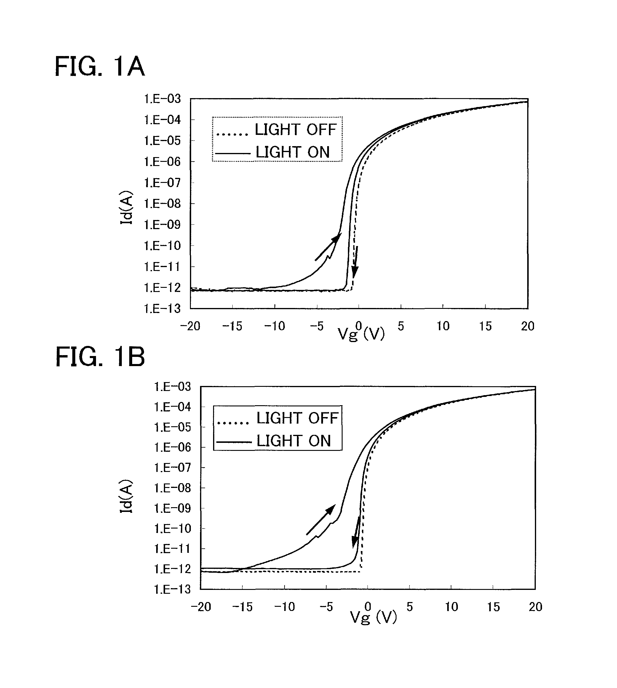
[0037]Described in Embodiment 1 is a relation between degradation with light irradiation to a transistor using an In—Ga—Zn—O-based oxide semiconductor which is a ternary metal oxide and hysteresis characteristics of the transistor.

[0038]First, results of a −BT test on a transistor (L / W=3 μm / 50 μm) using an In—Ga—Zn—O-based oxide semiconductor are shown in FIG. 10A. The −BT test was conducted at a drain-source voltage (Vd) of 3 V and a gate-source voltage (Vg) of −6 V such that the intensity of an electric field applied to a gate insulating film is −2 MV / cm. The application of the negative gate stress was kept for 0 seconds, 300 seconds, 1000 seconds, 3600 seconds, and 10000 seconds, Vg-Id curves for which showed that the Vg-Id curve shifts in a negative direction (a direction indicated by an arrow in FIG. 10A) as the kept time gets longer.

[0039]Further, results of the −BT test with light irradiation using an LED light source (white light with 36000 lux) are shown in FIG. 10B. As com...

embodiment 2

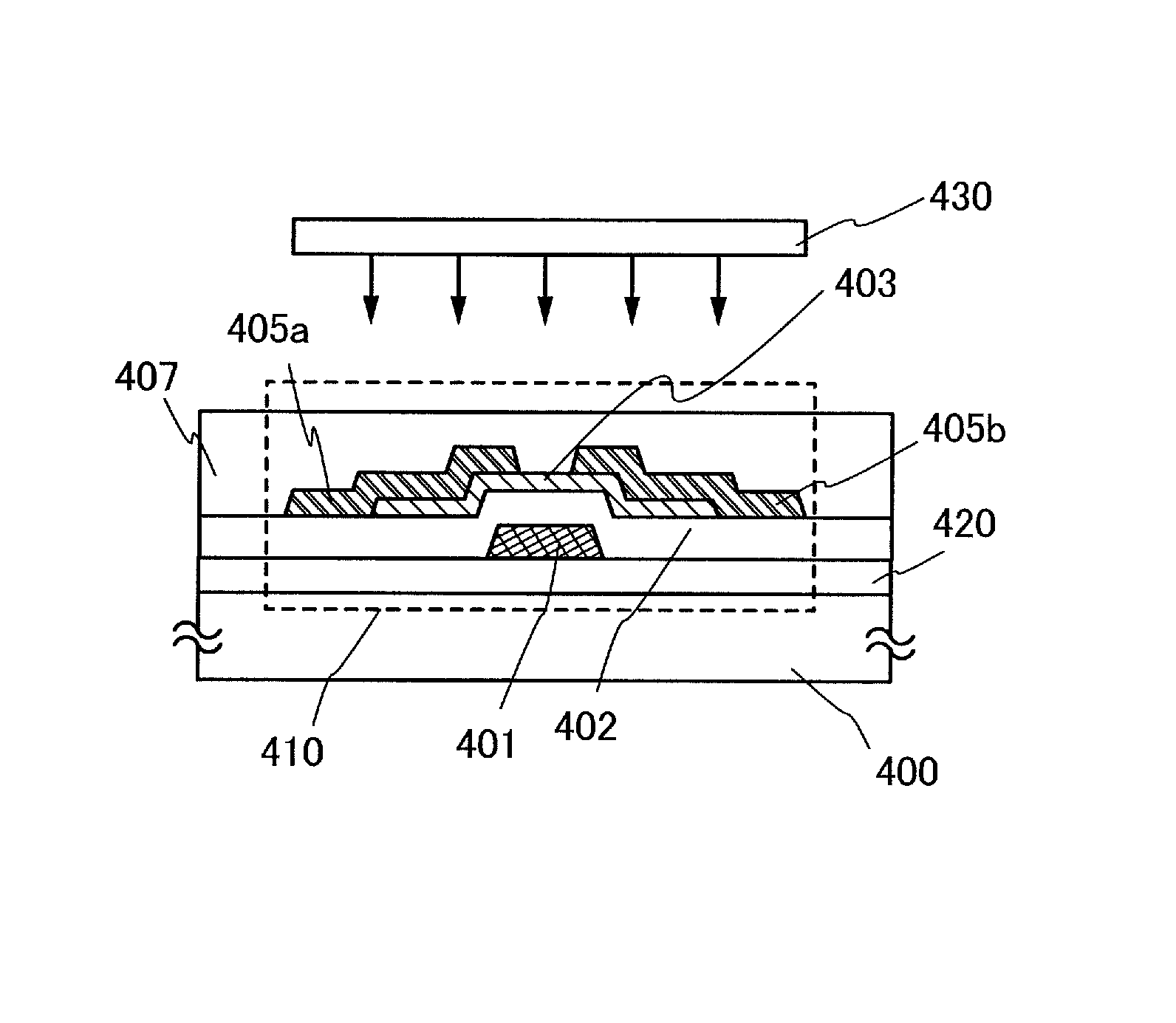
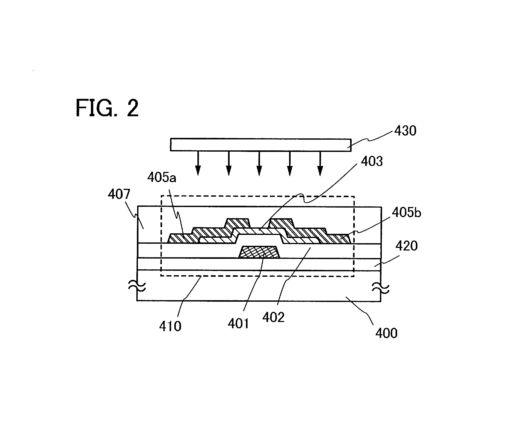
[0062]In Embodiment 2, an example of the case where a test using hysteresis characteristics is performed in a manufacturing process of a semiconductor device will be described.

[0063]An example of the manufacturing method of the transistor 410 is described using FIG. 2, below.

[0064]First, the insulating layer 420 serving as a base insulating layer is formed over the substrate 400. As the insulating layer 420, an insulating film including an inorganic insulating material is formed by a sputtering method, a PCVD method, or the like. Typically, an inorganic insulating film such as a silicon oxide film, a silicon oxynitride film, an aluminum oxide film, or a gallium oxide film can be used as the insulating layer 420.

[0065]Although there is no particular limitation on a material and the like of the substrate 400, it is necessary that the substrate have heat resistance high enough to withstand at least a heat treatment performed later. For example, a glass substrate, a ceramic substrate, a...


PUM


Abstract

Provided is a test method by which a transistor whose reliability is low can be detected with low stress and high accuracy in a shorter period of time than a BT test. Provided is to detect a transistor whose reliability is high in a shorter period of time than a BT test and manufacture an electronic device with high reliability efficiently. Hysteresis characteristics revealed in the result of the Vg-Id measurement with light irradiation to the transistor correlate with the result of a BT test; whether the reliability of the transistor is Good or Not-Good can be judged. Accordingly, the test method by which a transistor whose reliability is low can be detected with low stress and high accuracy in a shorter period of time than a BT test can be provided.

Description

BACKGROUND OF THE INVENTION[0001]1. Field of the Invention[0002]The present invention relates to a manufacturing method of a semiconductor device including a circuit including a transistor and a test method of the semiconductor device. The present invention relates to an electronic device equipped with a display device using an active element which is, for example, an active element including an oxide semiconductor, as a semiconductor element.[0003]In this specification, a semiconductor device generally means any device which can function by utilizing semiconductor characteristics; an electrooptic device, a semiconductor circuit, and an electronic device are all included in the category of the semiconductor device.[0004]2. Description of the Related Art[0005]Although transistors using amorphous silicon have been used for conventional display devices typified by liquid crystal televisions, an oxide semiconductor has attracted attention as a material which replaces a silicon semicondu...

Claims


Application Information

Patent Timeline
Patent Type & Authority Patents(United States)
IPC IPC(8): H01L21/00G01R31/311H01L21/84H01L21/66G01R31/26
CPCH01L22/14G01R31/311G01R31/2625H01L29/7869H01L29/66969
Inventor GODO, HIROMICHIYOSHITOMI, SHUHEI
Owner SEMICON ENERGY LAB CO LTD
Why Eureka
Try Eureka