Circuit system in a package

a technology of circuit system and electronic circuit, applied in the direction of semiconductor device details, semiconductor/solid-state device devices, electrical apparatus, etc., can solve the problems of increasing the number of external components, increasing the required board area and assembly expense, and complex frame shapes

Active Publication Date: 2015-03-31
SCI COMPONENTS
View PDF25 Cites 11 Cited by
  • Summary
  • Abstract
  • Description
  • Claims
  • Application Information

AI Technical Summary

Benefits of technology

[0016]It is yet another object of the present invention to provide an electronic circuit packaging system sealed against environmental contamination.
[0017]It is still another object of the present invention to provide an electronic circuit packaging system allowing the use of standard mass production techniques for both pc board arrays and lead frames.

Problems solved by technology

In some cases the lead frame shapes can be very complex.
However, the lead frame as a platform for electronic components works well only for integrated circuit dice and generally poorly for any other form of circuitry, thus increasing the number of external components needed to realize most specific circuit designs, and thus also increasing the required board area and assembly expense, and decreasing the circuit durability.
Additionally, the MLP is generally only designed to hold a single integrated circuit die.
A disadvantage of the SiP is the exposed via holes and exposed areas of the printed circuit board.
While this general type of invention provides improved means for preventing terminal pad pull-out, it is not designed to be capable of incorporating other electronic components to form a more complete functional circuit.
However, to avoid the problem of moisture infiltration the entire circuit portion of the assembly must be passivated with silicon nitride, a step requiring very specialized equipment and not cost-effective for many potential applications.
No means is taught for including discrete surface mount components or for protecting the printed circuit board.
Considerable effort has been expended to incorporate the protective circuitry as part of the integrated circuits rather than keeping it separate and no means is provided for including discrete surface mount components.
While this packaging system provides a means to combine both integrated circuit dice and surface mount components without the risk of moisture infiltration, the lead frame will require extensive configuring for any specific circuit application, and the resulting package will sit much higher than either a typical MLP or SiP package, undesirable for assembly density and miniaturization.

Method used


Image

  • Circuit system in a package
  • Circuit system in a package
  • Circuit system in a package

Examples


Embodiment Construction

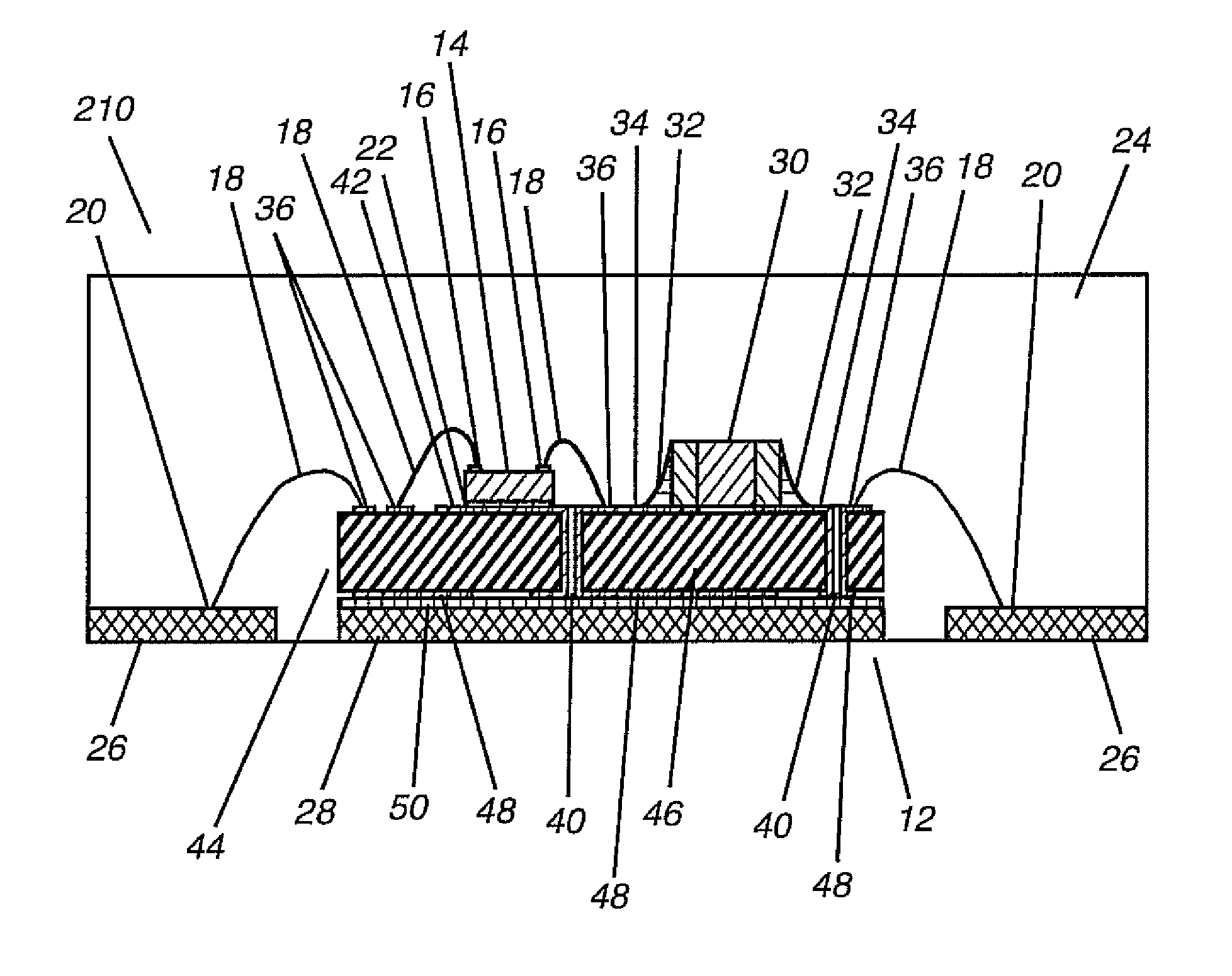
[0028]The present invention as taught herein is referred to as the MiniCircuits System in Package or MSiP, and is depicted in FIG. 3. The MSiP 210 includes many of the best features of both the MLP and SIP style of circuit packages with some novel improvements. A printed circuit board 44 is used to mount one or more integrated circuit dice 14 and surface mount components 30. The integrated circuit die 14 is attached to the die pad 28, typically with some form of die bonding adhesive 22, and wire bonds 18 are used to make electrical connection between the integrated circuit pads 16 and circuit board bonding pad areas 36. Surface mount components, which may include passive devices such as but not limited to resistors, capacitors, diodes and inductors, active devices such as but not limited to transistors, and even packaged surface mount circuits, are typically attached to the printed circuit board 44 using a conductive attachment material 32 which can be solder or conductive adhesive ...


PUM


Abstract

A circuit packaging system allows a combination of integrated circuit dice and surface mount electronic components to be mounted on a printed circuit board which is in turn mounted on a lead frame and encapsulated, thus providing an environmentally sealed package which is manufactured using standard circuit fabrication methods and machinery.

Description

BACKGROUND OF THE INVENTION[0001]1. Field of the Invention[0002]The present invention relates generally to a packaging system for electronic circuits, and more specifically to a packaging system wherein both integrated circuits and surface mount components are attached to a printed circuit board which is mounted on a lead frame and the circuit assembly is encapsulated.[0003]2. Description of the Prior Art[0004]Prior art circuit packaging systems include micro lead frame package (MLP) and system in package (SIP) assemblies. MLP are generally integrated circuit packages designed to be surface mounted. FIG. 1 shows a typical MLP 10, including a lead frame 12 preferably made of copper alloy, and a molded plastic body 24 to encapsulate the contents. FIG. 4 part A describes the basic manufacturing steps for an MLP 10. The lead frame 12 is produced in step A1 and is composed of several parts, mechanically joined by thin metal sections. Typically a lead frame 12 is composed of an outer fram...

Claims


Application Information

Patent Timeline
Patent Type & Authority Patents(United States)
IPC IPC(8): H01L23/495H01L23/06H01L21/48H01L23/00H01L23/31
CPCH01L21/4832H01L23/3107H01L24/97H01L2224/45144H01L2224/48091H01L2224/83005H01L23/3121H01L23/49513H01L23/49531H01L23/49589H01L21/561H01L21/568H01L24/29H01L24/32H01L24/48H01L24/73H01L24/83H01L24/85H01L24/92H01L2224/04042H01L2224/2929H01L2224/29339H01L2224/32225H01L2224/48227H01L2224/73265H01L2224/85444H01L2224/92247H01L2224/97H01L2924/19041H01L2924/19042H01L2924/19043H01L2924/19105H01L2924/19107H01L2224/85005H01L2224/48644H01L2924/181H01L2924/00014H01L2924/00012H01L2224/85H01L2224/83H01L2924/00H01L2224/45099H01L2224/45015H01L2924/207
Inventor KIEW, KELVIN K.
Owner SCI COMPONENTS
Why Eureka
Try Eureka