Semiconductor device

a semiconductor and device technology, applied in the direction of semiconductor devices, electrical devices, transistors, etc., can solve the problems of electrostatic discharge damage, gate insulating layer not providing excellent interface properties with the oxide semiconductor, and the mechanism of carrier generation in an oxide semiconductor is greatly different from that in a silicon-based semiconductor material, etc., to achieve stable electrical characteristics, prevent the effect of reducing the yield

Active Publication Date: 2015-06-02
SEMICON ENERGY LAB CO LTD
View PDF139 Cites 9 Cited by
  • Summary
  • Abstract
  • Description
  • Claims
  • Application Information

AI Technical Summary

Benefits of technology

[0010]For a semiconductor device including a transistor formed using a silicon-based semiconductor material such as amorphous silicon or polycrystalline silicon, a glass substrate of the eighth generation (2160 mm wide×2460 mm long) or later can be used. Thus, such a semiconductor device has advantages of high productivity and low cost. However, in the case of using such a glass substrate, because of its high insulating properties and large area, there arises the problem of electrostatic discharge (ESD) damage. This problem should inevitably be taken into consideration also in the case of using an oxide semiconductor material.
[0011]In view of such a technical background, an object of one embodiment of the present invention is to provide a highly reliable and electrically stable semiconductor device with a small number of changes in the transistor structure, the process conditions, the production apparatus, or the like from the mass production technology that has been put to practical use.
[0012]Another object of one embodiment of the present invention is to provide a semiconductor device the yield of which can be prevented from decreasing due to electrostatic discharge damage.
[0018]A semiconductor device according to one embodiment of the present invention is manufactured by a manufacturing method with a small number of changes from the mass production technology that has been put to practical use, and has stable electrical characteristics and high reliability.
[0019]In addition, according to one embodiment of the present invention, it is possible to provide a semiconductor device, the yield of which can be prevented from decreasing due to electrostatic discharge damage.

Problems solved by technology

However, the mechanism of carrier generation in an oxide semiconductor is greatly different from that in a silicon-based semiconductor material.
In particular, when a gate insulating layer used for the silicon-based semiconductor material is used for an oxide semiconductor, the gate insulating layer does not provide excellent interface properties with the oxide semiconductor.
However, in the case of using such a glass substrate, because of its high insulating properties and large area, there arises the problem of electrostatic discharge (ESD) damage.

Method used


Image

  • Semiconductor device
  • Semiconductor device
  • Semiconductor device

Examples


embodiment 1

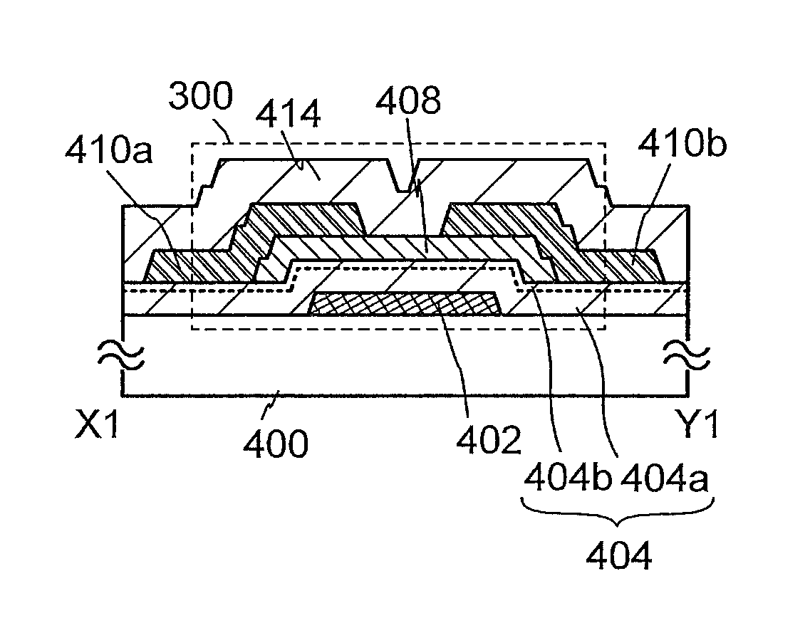
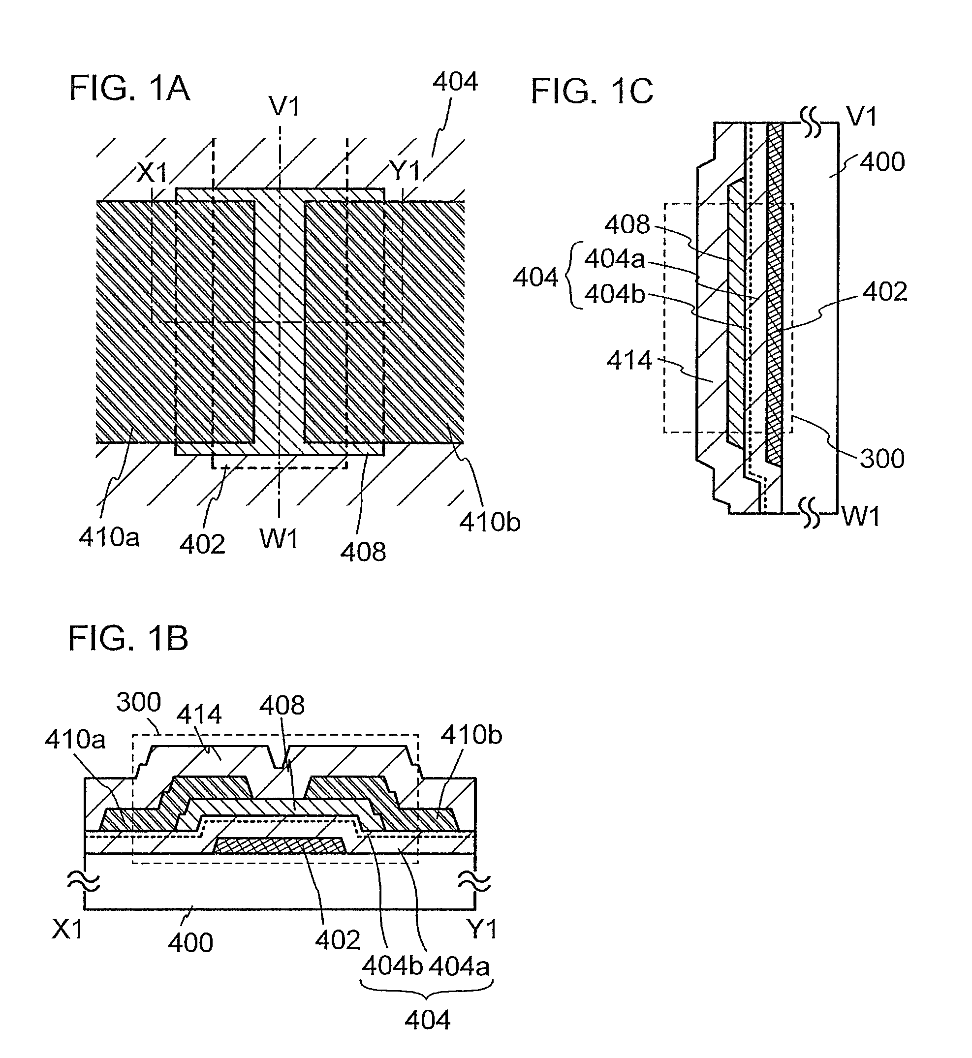
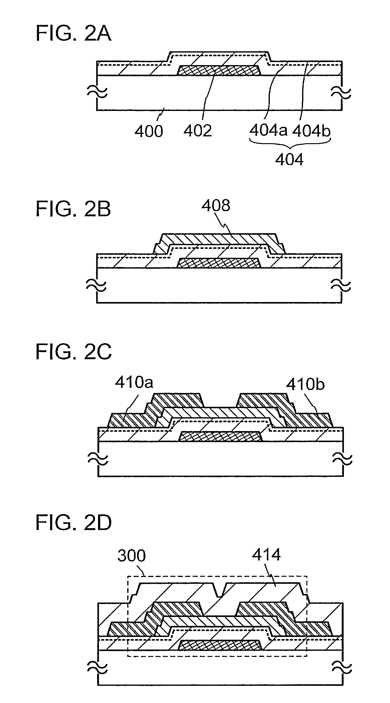
[0039]In this embodiment, embodiments of a semiconductor device and a method for manufacturing the semiconductor device will be described with reference to FIGS. 1A to 1C, FIGS. 2A to 2D, and FIGS. 3A to 3D. In this embodiment, bottom-gate transistors including oxide semiconductor layers are described as one example of a semiconductor device.

[0040]FIGS. 1A to 1C illustrate a structural example of a transistor 300. FIG. 1A is a plan view of the transistor 300, FIG. 1B is a cross-sectional view taken along the chain line X1-Y1 in FIG. 1A, and FIG. 1C is a cross-sectional view taken along the chain line V1-W1 in FIG. 1A.

[0041]The transistor 300 includes a gate electrode layer 402 over a substrate 400 having an insulating surface, a gate insulating layer 404 over the gate electrode layer 402, an oxide semiconductor layer 408 being above and in contact with the gate insulating layer 404 and overlapping with the gate electrode layer 402, and a source electrode layer 410a and a drain elect...

embodiment 2

[0151]A semiconductor device having a display function (also referred to as a display device) can be manufactured using any of the transistors described in Embodiment 1. Moreover, some or all of the driver circuits which include the transistor can be formed over a substrate where the pixel portion is formed, whereby a system-on-panel can be obtained.

[0152]In FIG. 4A, a sealant 4005 is provided so as to surround a pixel portion 4002 provided over a substrate 4001, and the pixel portion 4002 is sealed by using a substrate 4006. In FIG. 4A, a signal line driver circuit 4003 and a scan line driver circuit 4004 which are each formed using a single crystal semiconductor film or a polycrystalline semiconductor film on an IC or over a substrate separately prepared are mounted in a region that is different from the region surrounded by the sealant 4005 over the substrate 4001. Various signals and potentials are supplied to the pixel portion 4002 through the signal line driver circuit 4003 an...

embodiment 3

[0220]A semiconductor device having an image sensor function of reading information on an object can be manufactured using any of the transistors described in Embodiment 1.

[0221]FIG. 7A illustrates an example of a semiconductor device having an image sensor function. FIG. 7A is an equivalent circuit diagram of a photosensor, and FIG. 7B is a cross-sectional view illustrating part of the photosensor.

[0222]One electrode of a photodiode 602 is electrically connected to a photodiode reset signal line 658, and the other electrode of the photodiode 602 is electrically connected to a gate of a transistor 640. One of a source and a drain of the transistor 640 is electrically connected to a photosensor reference signal line 672, and the other of the source and the drain of the transistor 640 is electrically connected to one of a source and a drain of a transistor 656. A gate of the transistor 656 is electrically connected to a gate signal line 659, and the other of the source and the drain t...


PUM


Abstract

A highly reliable semiconductor device the yield of which can be prevented from decreasing due to electrostatic discharge damage is provided. A semiconductor device is provided which includes a gate electrode layer, a first gate insulating layer over the gate electrode layer, a second gate insulating layer being over the first gate insulating layer and having a smaller thickness than the first gate insulating layer, an oxide semiconductor layer over the second gate insulating layer, and a source electrode layer and a drain electrode layer electrically connected to the oxide semiconductor layer. The first gate insulating layer contains nitrogen and has a spin density of 1×10¹⁷ spins / cm3 or less corresponding to a signal that appears at a g-factor of 2.003 in electron spin resonance spectroscopy. The second gate insulating layer contains nitrogen and has a lower hydrogen concentration than the first gate insulating layer.

Description

TECHNICAL FIELD[0001]An embodiment of the invention disclosed in this specification and the like relates to a semiconductor device and a method for manufacturing the semiconductor device.[0002]In this specification and the like, a semiconductor device generally means a device which can function by utilizing semiconductor characteristics, and an electro-optical device, a light-emitting display device, a semiconductor circuit, and an electronic device are all semiconductor devices.BACKGROUND ART[0003]Attention has been focused on a technique for forming a transistor using a semiconductor thin film formed over a substrate having an insulating surface. The transistor is applied to a wide range of electronic devices such as an integrated circuit (IC) or an image display device (also simply referred to as a display device). A silicon-based semiconductor material is widely known as a material for a semiconductor thin film applicable to a transistor. As another material, an oxide semiconduc...

Claims


Application Information

Patent Timeline
Patent Type & Authority Patents(United States)
IPC IPC(8): H01L29/12H01L29/423H01L29/49H01L29/786
CPCH01L29/7869H01L29/42384H01L29/4908H01L29/40114H01L29/78606H01L29/495H01L29/513H01L29/518H01L29/78696H01L29/66742H01L29/66969
Inventor MIYAMOTO, TOSHIYUKINOMURA, MASAFUMIHAMOCHI, TAKASHIOKAZAKI, KENICHI
Owner SEMICON ENERGY LAB CO LTD
Why Eureka
Try Eureka