Material for organic electroluminescence device and electroluminescence device
a technology of electroluminescence device and material, which is applied in the direction of electroluminescent light source, chemistry apparatus and processes, and compositions. it can solve the problems of deterioration of device characteristics, inability to resist visible light, and complicated production steps or reduce productivity. , to achieve the effect of high blue color purity, easy oxidation, and high durability
- Summary
- Abstract
- Description
- Claims
- Application Information
AI Technical Summary
Benefits of technology
Problems solved by technology
Method used
Image
Examples
example 1
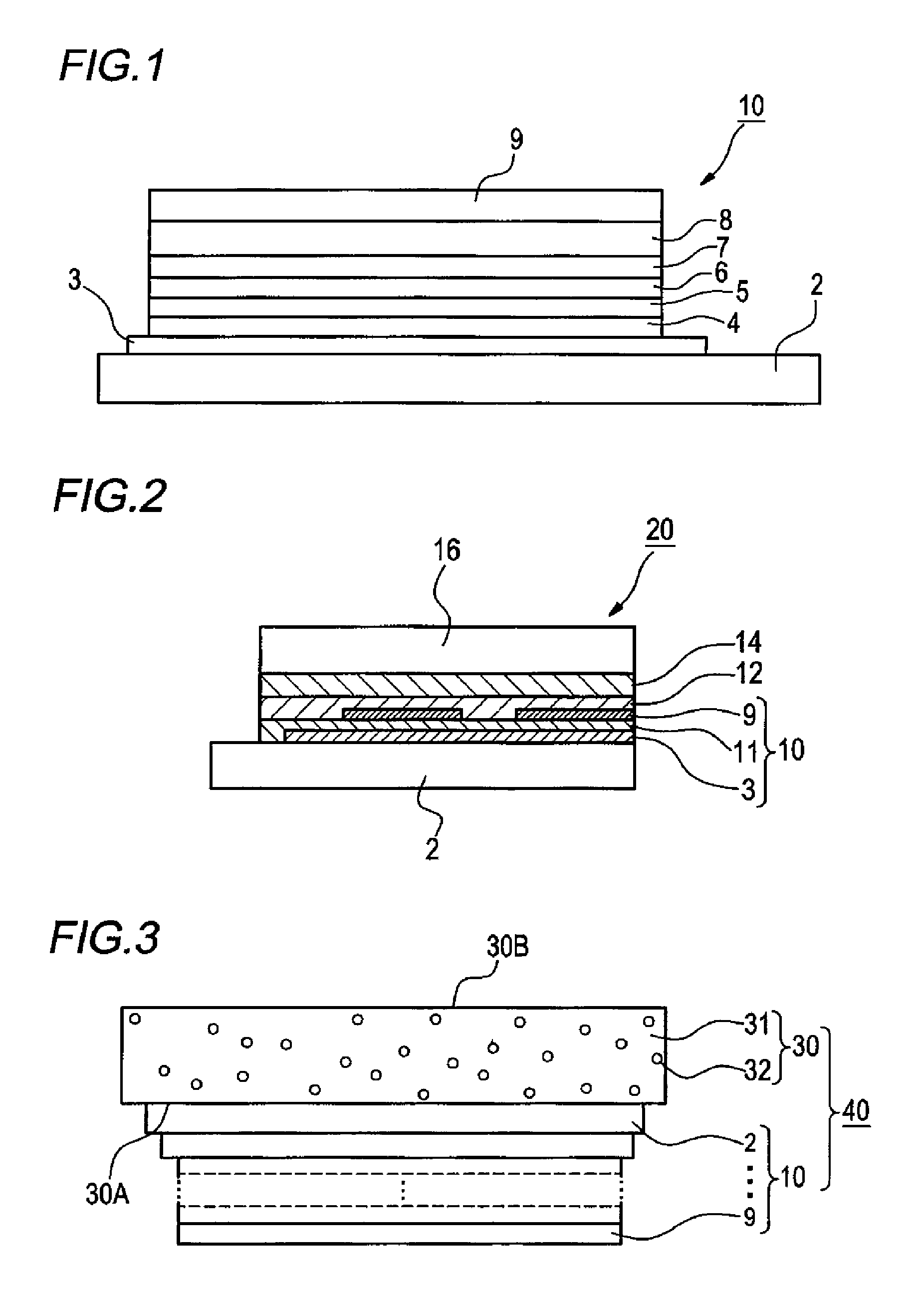
[0370]A glass substrate having an indium tin oxide (ITO) film of 100 μm thick and 2.5 cm square (manufactured by GEOMATEC, surface resistance: 10Ω / □) was placed in a washing vessel and ultrasonically washed in 2-propanol. Then, UV-ozone treatment was performed for 30 minutes. On the resulting transparent anode (ITO film), the following organic layers were successively deposited by using vacuum vapor deposition.
[0371]First layer: CuPc (copper phthalocyanine), film thickness: 120 nm
[0372]Second layer: NPD ((N,N′-di-α-naphthyl-N,N′-diphenyl)benzidine), 7 nm thick
[0373]Third layer: CBP (4,4′-di(9-carbazoyl)biphenyl)), film thickness: 3 nm
[0374]Fourth layer (light emitting layer): having Compound 1 (9 mass %) as a light emitting material (dopant) and mCBP (91 mass %) as a host material, film thickness: 30 nm
[0375]Fifth layer: first electron transport material (Balq): film thickness: 30 nm
[0376]A cathode was obtained by successively depositing, on the fifth layer, lithium fluoride and met...
example 2
[0388]Devices were prepared in a manner similar to that employed in Example 1 by using the light emitting materials shown in Table 6. Upon preparation, as soon as the materials were put in a crucible, vapor deposition was started (Vapor deposition condition 1).
[0389]Next, after the crucible containing the materials was heated for 48 hours without changing the temperature, vapor deposition was started (Vapor deposition condition 2) and a device was prepared similarly. Deposition condition 2 was performed on the assumption that a large amount of a material be vapor deposited successively upon production of devices. Brightness of the two devices thus prepared was measured by applying a voltage to give a current density of 10 mA / cm2. The brightness is expressed as a relative value supposing that the brightness of Device 2-1 is 100.
[0390]
TABLE 6Brightness underBrightness underDepositionvapor depositionLight emitting materialcondition 1condition 2(content ratio)(relative value)(relative v...
PUM
| Property | Measurement | Unit |
|---|---|---|
| dihedral angle | aaaaa | aaaaa |
| thickness | aaaaa | aaaaa |
| mass % | aaaaa | aaaaa |
Abstract
Description
Claims
Application Information


