Supercharge Your Innovation With Domain-Expert AI Agents!

Photovoltaic element

a photovoltaic element and photovoltaic energy technology, applied in the direction of photovoltaic energy generation, electrical equipment, semiconductor devices, etc., can solve the problems of high cost of technology, general limited proportion of light which can be used by dyes, and stability problems

Inactive Publication Date: 2015-07-21
BASF SE
View PDF35 Cites 9 Cited by
  • Summary
  • Abstract
  • Description
  • Claims
  • Application Information

AI Technical Summary

Benefits of technology

The present invention provides a photovoltaic element that has improved properties, especially in its p-semiconductor, even without the use of oxygen. This is achieved by using a silver in oxidized form, which can exist without oxygen for a long time. The element can be encapsulated to screen it from the surrounding atmosphere, protecting it from adverse effects of oxygen and other gases. The p-semiconductor can also be doped with other materials, such as organic matrices or organic light-emitting diodes, to further improve its properties. The invention also provides a process for producing the p-semiconductor and a dye solar cell using the improved elements.

Problems solved by technology

Even though silicon-based solar cells now dominate the market on Earth, this technology still remains costly.
However, the dye solar cell produced with liquid electrolyte in many cases suffers from nonoptimal sealing, which can lead to stability problems.
One disadvantage of the dye solar cell is that the proportion of light which can be used by the dye is generally limited by the energetic distance between the Fermi energies of the n- and p-conductors used.
The photovoltage is generally also limited by this distance.
In addition, dye solar cells generally have to be comparatively thin due to the charge transport required (for example 1-2.5 micrometers), such that the exploitation of the incident light is generally not optimal.
The result of this is that the fill factors of sDSCs are not very high, in particular at light intensities which are not low.
Even though the conductivity rises, the hole mobility was reduced as a result of the addition of the anions, which worsen the charge transport.
In addition, the stability of such antimony salts in the cells was questioned.
However, a decisive improvement in the sDSC cells was not achieved.
Components with organic dopants, however, have comparatively low lifetimes in many cases.
This doping too led to higher current efficiencies and energy efficiencies.
The storage of cells in an ambient atmosphere or in a controlled O2 atmosphere is, however, less reproducible and comparatively problematic with regard to commercial production of solar modules.
In addition, it is impossible to encapsulate oxygen-doped cells in an airtight manner, since a high conductivity of the whole conductor, which is needed for operation, is ensured only with constant contact to oxygen.

Method used


Image

  • Photovoltaic element
  • Photovoltaic element
  • Photovoltaic element

Examples


example 1

Doping with 5 mm AG-TFSI

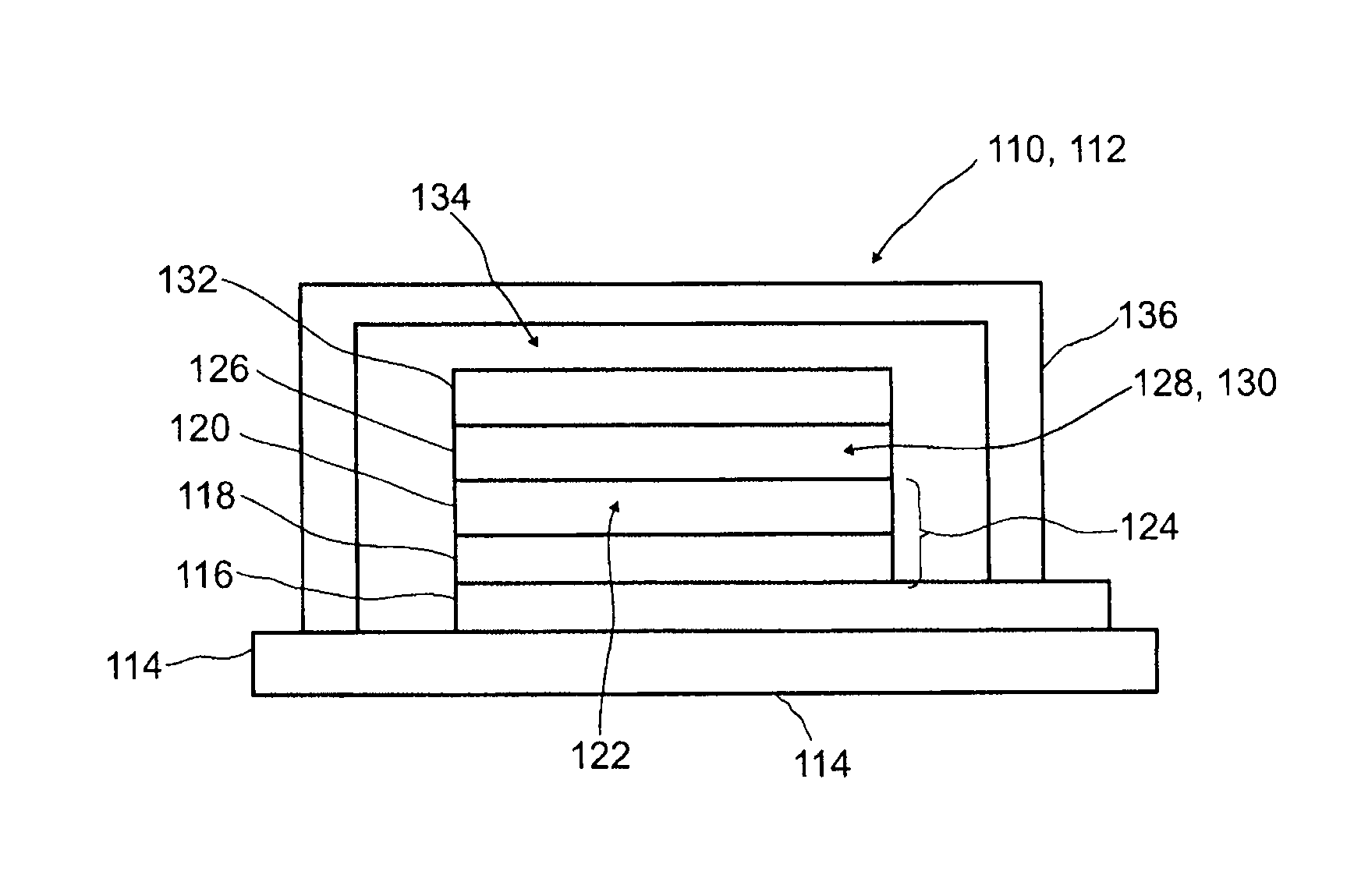
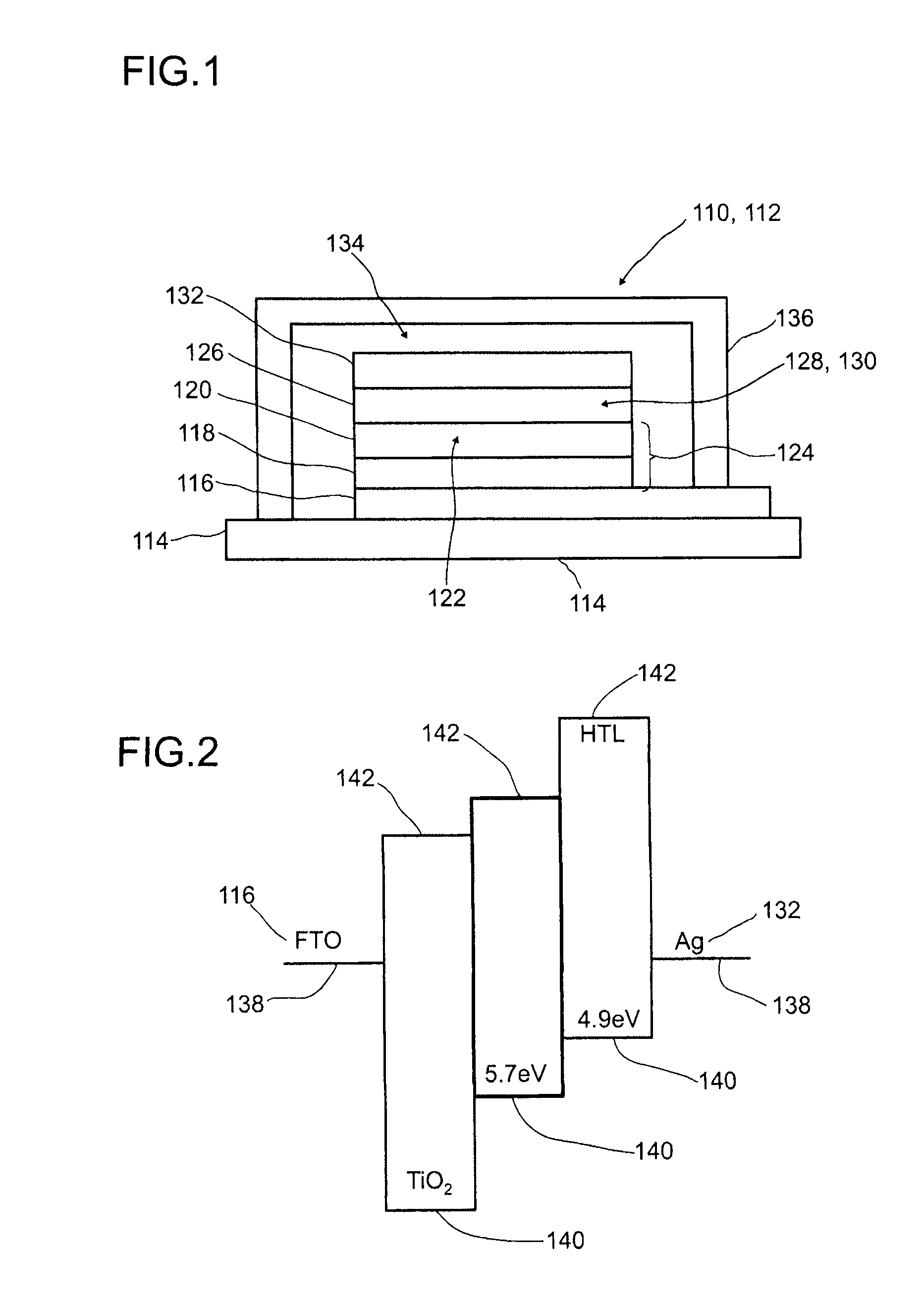
[0216]As the first working example of an inventive photovoltaic element 110, the above-described comparative sample was modified by doping the p-semiconductor 126 or the matrix material 128 thereof with silver bis(trifluoromethylsulfonyl)imide (Ag-TFSI). For this purpose, 5 mm silver bis(trifluoromethylsulfonyl)imide (source: Aldrich) in cyclohexanone was added to the p-semiconductor solution of 0.12M spiro-MeOTAD (source: Merck) and 20 mm LiN(BO2CF3)2 (source: Aldrich) in chlorobenzene. This solution was then spun onto the sample as described for the comparative sample.

[0217]The metal back electrode as the second electrode 132 was applied immediately thereafter by thermal metal vaporization under reduced pressure. The metal used was Ag, which was vaporized at a rate of 3 Å / s at a pressure of approx. 2*10−6 mbar so as to form a layer thickness of about 200 nm.

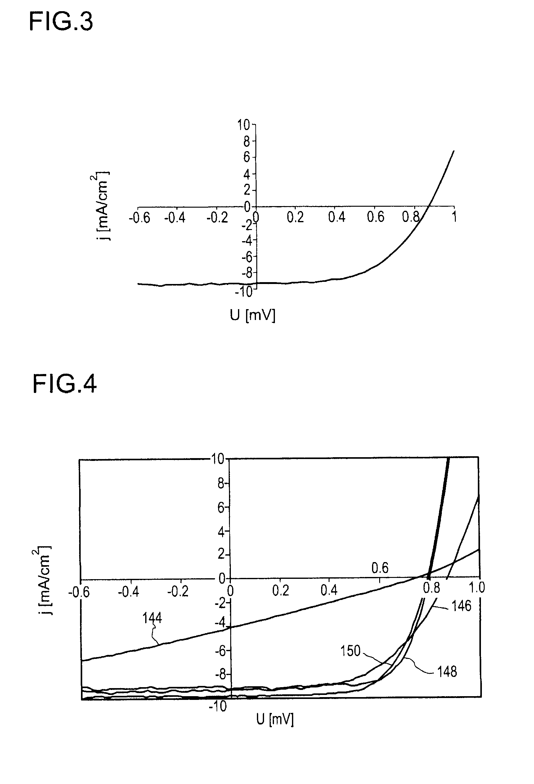
[0218]To determine the efficiency η, the particular current / voltage characteristic was measured with ...

example 2

Variation of the Dopant Concentration

[0221]In order to study the influence of the amount of dopant on the properties of the photovoltaic element 110, variations of example 1 were additionally produced with 1-20 mm silver bis(trifluoromethylsulfonyl)imide. Otherwise, the samples were produced like the sample according to the above-described example 1. The characteristics of these samples, measured after 2 days, are shown in table 3. The illumination in these measurements was in each case again 100 sun, as already in the measurements above.

[0222]

TABLE 3Comparison of characteristics of samples according to example 2 withdifferent Ag-TFSI content.Isc[mA / cm2]Voc[mV]FF[%]ETA[%] 1 mM Ag-TFSI−10.4780534.3 3 mM Ag-TFSI−10.1780624.8 5 mM Ag-TFSI−9.8780665.010 mM Ag-TFSI−9.7760695.120 mM Ag-TFSI−9.7800644.9

[0223]The measurements show that, in terms of efficiency, a maximum of approx. 5.1% occurs at approx. 10 mm Ag-TFSI. Overall, the efficiency between 3 mm and 20 mm, however, follows a compar...

example 3

Variation of the Matrix Material

[0224]In addition, as example 3, the influence of the matrix material 128 on the properties of the photovoltaic elements 110 was studied. For this purpose, samples were produced according to the above-described example 1, except that spiro-MeOTAD as matrix material 128 was replaced by different matrix materials 128 with different concentrations, more particularly by the matrix materials of the ID522, ID322 and ID367 types already mentioned above. To introduce silver 130 in oxidized form, the dopant used was again in each case 10 mm silver bis(trifluoromethylsulfonyl)imide in all samples. The characteristics of the samples obtained in this way are shown in table 4. The specified concentrations of 160 mg / ml and 200 mg / ml are based on the concentration of the matrix material 128 in the liquid phase. The characteristics were again recorded after 2 days and measured at 100 sun [mW / cm2].

[0225]

TABLE 4Comparison of characteristics of samples according to exam...


PUM


Abstract

A photovoltaic element (110) is proposed for conversion of electromagnetic radiation to electrical energy, more particularly a dye solar cell (112). The photovoltaic element (110) has at least one first electrode (116), at least one n-semiconductive metal oxide (120), at least one electromagnetic radiation-absorbing dye (122), at least one solid organic p-semiconductor (126) and at least one second electrode (132). The p-semiconductor (126) comprises silver in oxidized form.

Description

FIELD OF THE INVENTION[0001]The invention relates to a photovoltaic element, to a process for production of a solid organic p-semiconductor for use in an organic component, and to a process for production of a photovoltaic element. Such photovoltaic elements and processes are used to convert electromagnetic radiation, especially sunlight, to electrical energy. More particularly, the invention can be applied to dye solar cells.STATE OF THE ART[0002]The direct conversion of solar energy to electrical energy in solar cells is based generally on what is called the “internal photo effect” of a semiconductor material, i.e. the production of electron-hole pairs by absorption of photons and the separation of the negative and positive charge carriers at a p-n junction or a Schottky contact. In this way, a photovoltage is generated, which, in an external circuit, can cause a photocurrent through which the solar cell releases its power. The semiconductor can generally only absorb those photons...

Claims


Application Information

Patent Timeline
Patent Type & Authority Patents(United States)
IPC IPC(8): H01L31/042H01L51/00H01L51/42H01L31/0256H10K99/00
CPCH01L51/002H01L51/4226H01L31/0256H01L51/006H01L51/0053H01L51/0059H01L2031/0344Y02E10/549H10K71/30H10K85/621H10K85/631H10K85/633H10K30/151H10K30/50
Inventor KUHN, ALFREDBRUDER, INGMARSENS, RUDIGERPSCHIRER, NEIL GREGORYERK, PETER
Owner BASF SE
Features
  • R&D
  • Intellectual Property
  • Life Sciences
  • Materials
  • Tech Scout
  • Unparalleled Data Quality
  • Higher Quality Content
  • 60% Fewer Hallucinations
Learn More