Methods for construction and optimization of a clock tree plan for reduced power consumption

a clock tree and power consumption technology, applied in the direction of instruments, software simulation/interpretation/emulation, generating/distributing signals, etc., can solve the problems of increasing common over-aggressive gating, inconvenient estimating of inability to accurately predict timing and power during automatic clock gate insertion, etc., to achieve the effect of improving timing and power consumption, and facilitating the modeling of clock buffers with respect to clock gates

Active Publication Date: 2015-09-15
CADENCE DESIGN SYST INC
View PDF24 Cites 45 Cited by
  • Summary
  • Abstract
  • Description
  • Claims
  • Application Information

AI Technical Summary

Benefits of technology

[0011]After the clock buffers, enable gates, clock gates, and clocked elements are placed within a floor plan, the clock tree plan does not need to follow the clock tree prototype and can be altered to optimize the physical placement of the clock buffers, enable gates, clock gates, and clocked elements to improve timing and power consumption. After placement in a floorplan, clocked elements in the clock tree plan can be optimized such as by merging clock subtrees at merger points or cloning clock gates for insertion into branches of a clock subtree.
[0014]Another aspect of the embodiments of the invention is that physical placement is considered during the clock tree planning process. Another aspect of the embodiments of the invention is cluster placement of clocked elements in portions of the integrated circuit design. Cloning of clock gates or clock buffers, one or more times, may be used to improve timing and / or power consumption in one or more branches of clock signal paths within a clock subtree that lead to the clusters of clocked elements. The placement of buffers and clock gates in the clock tree is evaluated to optimize power and balance timing.
[0015]Another aspect of the embodiments of the invention is a merger algorithm that is used to evaluate merging of clock trees, clock gates, and clocked elements in the formation of an optimized clock tree plan. The merger algorithm is a bottom up recursive binary merging algorithm. A partial tree model of clock subtrees (a gate model, timing model, energy / power model) may be created to determine whether or not to merge. The partial tree models are recursively built as you move up the hierarchy towards the clock source at a clock generator. At every stage of hierarchy, a history of the lower level clock subtrees and clocked elements is maintained. The goal of the merger algorithm is to conserver maximum power while meeting timing requirements. To do so, the merger algorithm evaluates cost functions of potential mergers of clock subtrees. It evaluates power consumption / conservation, enable timing, signal skew, and data timing delay of the potential mergers of clock subtrees. With a merger, redundancy is avoided to reduce power consumption. Clock signal skew is balanced to avoid race conditions. Clock signal timing is balanced with data signal timing at a flip flop to assure capture of data while gating clock signals to conserver power.

Problems solved by technology

Clock synthesis is often considered at the end of the design even though decisions made in the front-end design flow of an integrated circuit may have significant consequences on the subsequent timing and power closure of the clock design and its clock tree.
For low power integrated circuit designs, estimating the costs of timing and power during automatic clock gate insertion is imprecise with such late clock synthesis.
However, with the availability of advanced functional gating techniques, overly aggressive gating is an increasingly common result.
Another negative consequence of clock synthesis occurring late in the design flow is the greater difficulty of grouping and cloning clock signals, such that it does not correspond to the physical netlist.
With clock synthesis occurring later in the design flow, it may be more difficult to obtain timing closure of the integrated circuit design during clock tree synthesis.

Method used


Image

  • Methods for construction and optimization of a clock tree plan for reduced power consumption
  • Methods for construction and optimization of a clock tree plan for reduced power consumption
  • Methods for construction and optimization of a clock tree plan for reduced power consumption

Examples


Embodiment Construction

[0064]In the following detailed description of the embodiments of the invention, numerous specific details are set forth in order to provide a thorough understanding of the present invention. However, it will be obvious to one skilled in the art that the embodiments of the invention may be practiced without these specific details. In other instances well known methods, procedures, components, and circuits have not been described in detail so as not to unnecessarily obscure aspects of the embodiments of the invention.

[0065]Note also that the terms flip-flop and register are being used interchangeably herein. That is, each reference to a flip-flop herein also means a register of a plurality of flip-flops that are clocked together by the same clock signal. In a register, each flip flop typically has a data input coupled to a respective data signal to store data bits from a bus of parallel data signals. Accordingly, a reference to a flip-flop herein also means a register of a plurality ...


PUM


Abstract

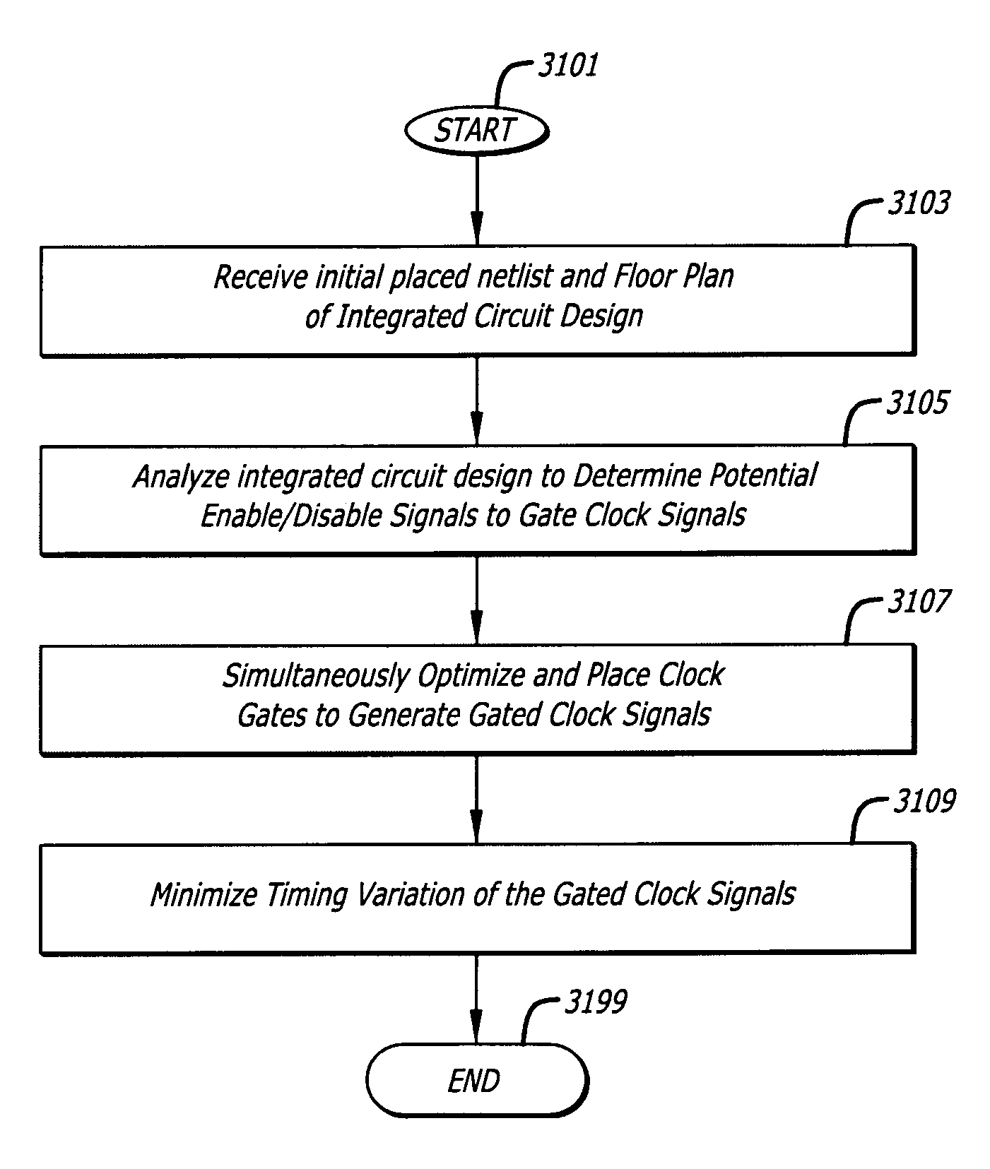
In one embodiment of the invention, a method of physical clock topology planning for designing integrated circuits is disclosed. The method includes reading an initial placed netlist of an integrated circuit design and a floorplan of the integrated circuit design, analyzing the integrated circuit design to determine potential enable signals to gate clock signals that clock the plurality of flip flops to reduce power consumption; simultaneously optimizing and placing the clock enable logic gates to gate clock signals to the plurality of flip flops; and minimizing timing variation of the clock signals to the plurality of flip flops.

Description

CROSS REFERENCE[0001]This non-provisional United States (U.S.) patent application claims the benefit of U.S. Provisional Patent Application No. 61 / 732,284 filed on Nov. 30, 2012 by inventors Ankush Sood, et al., entitled GRAPHICAL USER INTERFACE FOR PHYSICALLY AWARE CLOCK TREE PLANNING, incorporated herein by reference.[0002]This application is also related to U.S. patent application Ser. No. 13 / 732,364 filed on Dec. 31, 2012 by inventors Tsuwei Ku, et al., entitled PHYSICALLY AWARE LOGIC SYNTHESIS OF INTEGRATED CIRCUIT DESIGNS, incorporated herein by reference.FIELD[0003]The embodiments of the invention relate generally to clock tree topology planning for designing integrated circuits.BACKGROUND[0004]Digital circuits within integrated circuit chips are often synchronized by one or more clock signals. Data is periodically stored in registers that are clocked by such clock signals. When data is not being evaluated, it is desirable to control or gate the clocks to unused circuitry in ...

Claims


Application Information

Patent Timeline
Patent Type & Authority Patents(United States)
IPC IPC(8): G06F17/50G06F9/455
CPCG06F17/50G06F17/5072G06F30/396G06F1/10G06F2119/12G06F30/327G06F30/392G06F30/394G06F30/3312G06F30/00
Inventor SOOD, ANKUSHHURST, AARON PAUL
Owner CADENCE DESIGN SYST INC
Why Eureka
Try Eureka