Supercharge Your Innovation With Domain-Expert AI Agents!

Compliant printed circuit wafer level semiconductor package

a technology of printed circuit wafers and semiconductor packages, applied in semiconductor devices, semiconductor/solid-state device details, electrical apparatus, etc., can solve the problems of device not being connected to the final pcb, size and distance between die terminals is so small, and achieves the effect of improving electrical performan

Active Publication Date: 2015-09-15
HSIO TECH
View PDF427 Cites 13 Cited by
  • Summary
  • Abstract
  • Description
  • Claims
  • Application Information

AI Technical Summary

Benefits of technology

The present patent is about a new semiconductor package design that uses additive printing processes instead of traditional methods. This allows for the direct writing of circuitry and dielectrics, with added benefits like stress decoupling and embedded function. The use of additive printing processes also allows for a wider variety of materials to be applied on a layer with a registration relative to the previous layer, which improves electrical performance. The semiconductor package can also be produced as a "Green" product, with reduced environmental issues. Additionally, the patent discusses several additive processes that combine the mechanical or structural properties of a polymer material, while adding metal materials in an unconventional fashion, to create electrical paths that improve electrical performance. Overall, the new semiconductor package design offers improved performance, reduced cost, and environmental friendliness.

Problems solved by technology

In many cases, the size and distance between die terminals is so small that the device cannot be connected to the final PCB without some sort of fan out or routing.
In many cases, the size and distance between die terminals is so small that the IC device cannot be connected to the final PCB without some sort of re-routing interface.
In both cases, the connection of the IC device to the package is generally not reworkable once packaged and if there is a missing or broken connection it is difficult to repair.
In many cases, the functional performance of the IC device is not known prior to placing it into the package and if the packaged IC device fails testing the cost of the package and processing is lost.
In general, the area array packaging is more expensive due to the larger pin counts and more sophisticated substrates required.
The main limitations for area array packaging are the terminal pitch, thermal management, cost, ability to rework faulty IC devices and reliability of the solder joints.

Method used


Image

  • Compliant printed circuit wafer level semiconductor package
  • Compliant printed circuit wafer level semiconductor package
  • Compliant printed circuit wafer level semiconductor package

Examples


Embodiment Construction

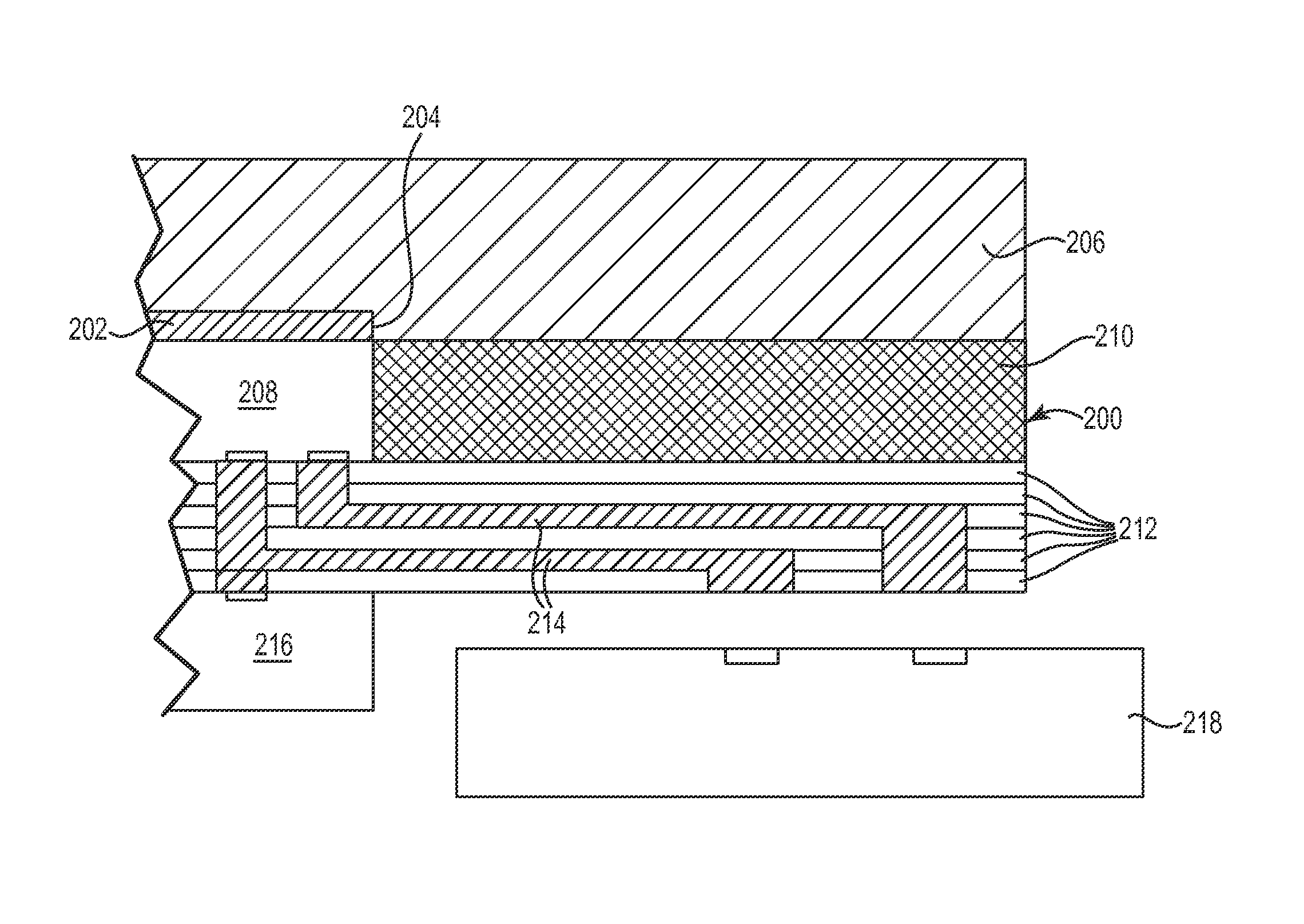
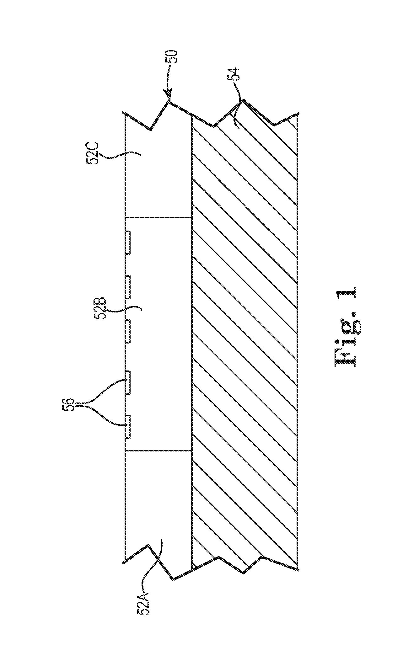
[0038]FIG. 1 is a side sectional view of semiconductor wafer 50 containing a plurality of IC devices 52A, 52B, 52C (collectively “52”) located on substrate 54. The IC terminals 56 are facing up. The substrate 54 may be a temporary work surface or may be a portion of the final semiconductor package. The substrate 54 can be constructed from a variety of rigid or flexible polymeric materials, such as for example, UV stabilized tetrafunctional epoxy resin systems referred to as Flame Retardant 4 (FR-4); bismaleimide-triazine thermoset epoxy resins referred to as BT-Epoxy or BT Resin; and liquid crystal polymers (LCPs), which are polyester polymers that are extremely unreactive, inert and resistant to fire. Other suitable plastics include phenolics, polyester (PET), polyimide (PI), polyethylene napthalate (PEN), Polyetherimide (PEI), along with various fluoropolymers (FEP) and copolymers, and Ryton® available from Phillips Petroleum Company. For some applications, the substrate 54 can be...


PUM


Abstract

A wafer-level package for semiconductor devices and a method for making the package. At least one dielectric layer is selectively printed on at least a portion of the semiconductor devices creating first recesses aligned with a plurality of electrical terminals on the semiconductor devices. A conductive material is printed in the first recesses to form contact members on the semiconductor devices. At least one dielectric layer is selectively printed to create a plurality of second recesses corresponding to a target circuit geometry. A conductive material is printed in at least a portion of the second recesses to create a circuit geometry. The circuit geometry includes a plurality of exposed terminals adapted to electrically couple to another circuit member. The wafer is diced to provide a plurality of discrete packaged semiconductor devices.

Description

CROSS-REFERENCE TO RELATED APPLICATIONS[0001]This application is a national stage application under 35 U.S.C. §371 of International Application No. PCT / US2010 / 036288, titled COMPLIANT PRINTED CIRCUIT WAFER LEVEL SEMICONDUCTOR PACKAGE, filed May 27, 2010, which claims priority to U.S. Provisional Application No. 61 / 183,356, filed Jun. 2, 2009, both of which are hereby incorporated by reference in their entireties.TECHNICAL FIELD[0002]The present application is directed to leveraging the capabilities of additive printing processes to provide a wafer level semiconductor package that results in a high performance packaged IC devices after wafer dicing.BACKGROUND OF THE INVENTION[0003]Traditional semiconductors and IC devices are typically packaged in a variety of ways to provide redistribution from the terminals on the die to a spacing that is conducive to cost effective printed circuit board (“PCB”) fabrication techniques. In many cases, the size and distance between die terminals is s...

Claims


Application Information

Patent Timeline
Patent Type & Authority Patents(United States)
IPC IPC(8): H01L23/538H01L23/31H01L21/683H01L25/065H01L23/00H01L23/525
CPCH01L23/3114H01L21/6836H01L23/5389H01L24/20H01L25/0657H01L23/525H01L24/03H01L24/11H01L24/13H01L24/94H01L2221/68372H01L2224/024H01L2224/0236H01L2224/02335H01L2224/0401H01L2224/04105H01L2224/0557H01L2224/1147H01L2224/11334H01L2224/20H01L2224/94H01L2225/06541H01L2924/0002H01L2924/00014H01L2924/01004H01L2924/014H01L2924/01006H01L2924/01013H01L2924/01015H01L2924/01029H01L2924/01033H01L2924/01046H01L2924/01047H01L2924/01049H01L2924/01075H01L2924/01078H01L2924/01079H01L2924/01082H01L2924/01087H01L2924/09701H01L2924/12044H01L2924/1306H01L2924/14H01L2924/19041H01L2924/3011H01L2924/3025H01L2224/03H01L2224/11H01L2924/00H01L2224/05552
Inventor RATHBURN, JAMES
Owner HSIO TECH
Features
  • R&D
  • Intellectual Property
  • Life Sciences
  • Materials
  • Tech Scout
  • Unparalleled Data Quality
  • Higher Quality Content
  • 60% Fewer Hallucinations
Learn More