Storage element, storage device, method of manufacturing storage element, and magnetic head

a technology of storage elements and magnetic heads, which is applied in the direction of digital storage, magnetic field-controlled resistors, instruments, etc., can solve the problems of reducing the magnetic resistance ratio of the element, difficult storage operation in the range of operation voltages, etc., and achieves effective function, excellent storage characteristics, and low resistance in the element.

Active Publication Date: 2016-07-19
SONY CORP
View PDF6 Cites 3 Cited by
  • Summary
  • Abstract
  • Description
  • Claims
  • Application Information

AI Technical Summary

Benefits of technology

[0041]In so doing, it is possible to generate a region with a low resistance value as a portion of the spin barrier layer.
[0042]According to the embodiments of the technology, it is possible to lower the resistance in the element while causing interface magnetization anisotropy to effectively function due to the spin barrier layer in a storage element having two oxide films of a tunnel barrier layer and spin barrier layer on both surface sides of a storage layer, and realize a storage element with excellent storage characteristics and which is able to operate at low power.

Problems solved by technology

Therefore, the resistance of the element is raised by providing a spin barrier layer, and the storage operation becomes difficult in the range of operation voltages.
Furthermore, since the spin barrier layer does not have magnetic resistance, there is a hindrance when reading out information for which the magnetic resistance ratio of the element is decreased.

Method used


Image

  • Storage element, storage device, method of manufacturing storage element, and magnetic head
  • Storage element, storage device, method of manufacturing storage element, and magnetic head
  • Storage element, storage device, method of manufacturing storage element, and magnetic head

Examples


first to twelfth embodiments

[0163]Next, a specific configuration of the storage element 3 of the embodiment will be described as first to twelfth embodiments.

[0164]The storage element 3 of the first to twelfth embodiments basically includes an underlayer 14, a magnetization fixing layer 15, a tunnel barrier layer 16, a storage layer 17, a spin barrier layer 18, and an electrode layer 19, similarly to the layer structure shown in FIG. 3B. In particular, by arranging the tunnel barrier layer 16 and the spin barrier layer 18 as oxide layers on both sides of the storage layer 17, the configuration obtains strong interface magnetization anisotropy.

[0165]The spin barrier layer 18 has an effect in which the storage characteristics of information are improved by improving the coercive force of the storage layer 17, and an effect in which the efficiency of the spin torque is improved. Therefore, the spin barrier layer 18 is effective in order to prepare a magnetic memory with low power consumption at a high density.

[01...

second and third embodiments

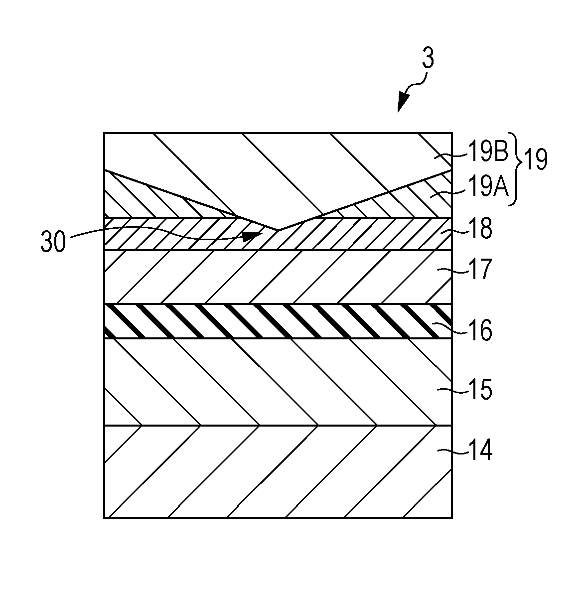
[0170]FIG. 3A shows the layer structure of the storage element 3 of the first embodiment. As depicted in the drawing, the underlayer 14, the magnetization fixing layer 15, the tunnel barrier layer 16, the storage layer 17, the spin barrier layer 18 and the electrode layer 19 are included. The electrode layer 19, for example, is configured by a first electrode layer 19A and the second electrode layer 19B made from different materials.

[0171]In this case, although the spin barrier layer 18 is formed with a predetermined set film thickness value (for example, a film thickness value of 0.6 nm or more and 0.7 nm or less), a low resistance region 30 is formed in a portion (peripheral region of the film surface) of the spin barrier layer 18.

[0172]In this case, the low resistance region 30 is a region in which the film thickness value of a portion (center region) of the spin barrier layer 18 is a lower value than the set film thickness value, and, more specifically, is a region in which the ...

embodiment

Method of Manufacturing of Sixteenth Embodiment

[0263]Next, the method of manufacturing of the sixteenth embodiment in which the spin barrier layer 18 is formed by etching after etching of the first electrode layer 19A will be described with FIG. 12.

[0264]Since the steps shown in FIGS. 9A to 9F as the fourteenth embodiment are the same, description will not be made.

[0265]After entering the state in FIG. 9F, etching is performed by ion beam irradiation from an oblique direction as in FIG. 12A.

[0266]At this time, if the etching method, type and conditions of gas, and the like are selected so as to selectively etch the material of the first electrode layer 19A, it is possible to remove the end portion of the first electrode layer 19A without excessively removing the spin barrier layer 18, and thereby possible for the spin barrier layer 18 to be exposed.

[0267]Next, etching is performed by ion beam irradiation from above as in FIG. 12B. In this case, the etching rate of the first electrod...


PUM


Abstract

A storage element includes a layer structure, which includes a storage layer including magnetization perpendicular to the film surface, in which the magnetization direction is changed corresponding to information; a magnetization fixing layer including magnetization perpendicular to the film surface that becomes a reference for information stored on the storage layer; a tunnel barrier layer made from an oxide provided between the storage layer and the magnetization fixing layer; and a spin barrier layer made from an oxide provided contacting the surface of the opposite side of the storage layer to the surface contacting the tunnel barrier layer. A low resistance region is formed in a portion of the spin barrier layer formed with a predetermined set film thickness value and information storage on the storage layer is performed by changing the magnetization direction of the storage layer by current flowing in the stacking direction of the layer structure.

Description

CROSS REFERENCES TO RELATED APPLICATIONS[0001]The present application claims priority to Japanese Priority Patent Application JP 2013-126388 filed in the Japan Patent Office on Jun. 17, 2013, the entire content of which is hereby incorporated by reference.BACKGROUND[0002]The present application relates to a storage element that includes a plurality of magnetic layers and performs recording using spin-torque magnetization reversal, a storage device including the storage element, a manufacturing method of the storage element, and further, a magnetic head including the storage element.[0003]Although a high density dynamic random access memory (DRAM) that operates at high speeds is widely used in information devices, such as computers, as a random access memory, there is strong demand for a non-volatile memory as a memory that replaces the DRAM, which is a volatile memory, or as a memory that is used with the DRAM or the like. Magnetic random access memory (MRAM) that records informatio...

Claims


Application Information

Patent Timeline
Patent Type & Authority Patents(United States)
IPC IPC(8): H01L43/02H01L43/12H01L43/08H01L27/22G11C11/16
CPCH01L43/12H01L43/08G11C11/161H01L27/228H10B61/22H10N50/01H10N50/10
Inventor OHMORI, HIROYUKIHOSOMI, MASANORIBESSHO, KAZUHIROHIGO, YUTAKAYAMANE, KAZUTAKAUCHIDA, HIROYUKI
Owner SONY CORP
Why Eureka
Try Eureka