Dispersion model for band gap tracking

a dispersion model and band gap technology, applied in the direction of individual semiconductor device testing, semiconductor/solid-state device testing/measurement, instruments, etc., can solve the problems of measurement technology suffering from any of a number of limitations, measurement requires the destruction of samples, measurement accuracy is not high, etc., to achieve accurate characterization of band gaps and gain insight and control over a manufacturing process.

Active Publication Date: 2017-03-14
KLA TENCOR TECH CORP
View PDF5 Cites 18 Cited by
  • Summary
  • Abstract
  • Description
  • Claims
  • Application Information

AI Technical Summary

Benefits of technology

[0016]Methods and systems for determining band structure characteristics of high-k dielectric films deposited over a substrate based on spectral response data are presented. Optical models of semiconductor structures such as gate dielectric stacks are presented. In particular, models capable of accurate characterization of band gap in high-K dielectric layers and nanostructures based on high-K dielectric materials are described. These models quickly and accurately represent experimental results in a physically meaningful manner that can be subsequently used to gain insight and control over a manufacturing process.

Problems solved by technology

Currently, however, these measurement technologies suffer from any of a number of limitations.
In some cases, the measurements require destruction of the sample.
In some cases, the measurement technology is slow, and must be separated from the production line.
However, direct inversion methods are computationally burdensome, very sensitive to statistical measurement errors, and do not provide a physically based model of the measured structure (i.e., the optical functions do not satisfy the Kramers-Kronig consistency condition).
As a result, the utility of direct inversion methods for high-throughput inspection and process control is limited.
In addition, the direct inversion method involves an ill-defined mathematical problem.
For these practical reasons, both BEMA and direct inversion are limited in their ability to accurately monitor band gap.
An important limitation of the conventional Cody-Lorentz function is that it has discontinuous derivatives over the energy range, E, and the resonant energy range, E0, at the Urbach transition energy level, ET.
This leaves the dispersion model mathematically ill-defined, leaving open the possibility that the model will yield results that have no relation to real, physical features of the material.
In particular, a discontinuity of derivatives may make the optimization process computationally unstable.

Method used


Image

  • Dispersion model for band gap tracking
  • Dispersion model for band gap tracking
  • Dispersion model for band gap tracking

Examples


Embodiment Construction

[0028]Reference will now be made in detail to background examples and some embodiments of the invention, examples of which are illustrated in the accompanying drawings.

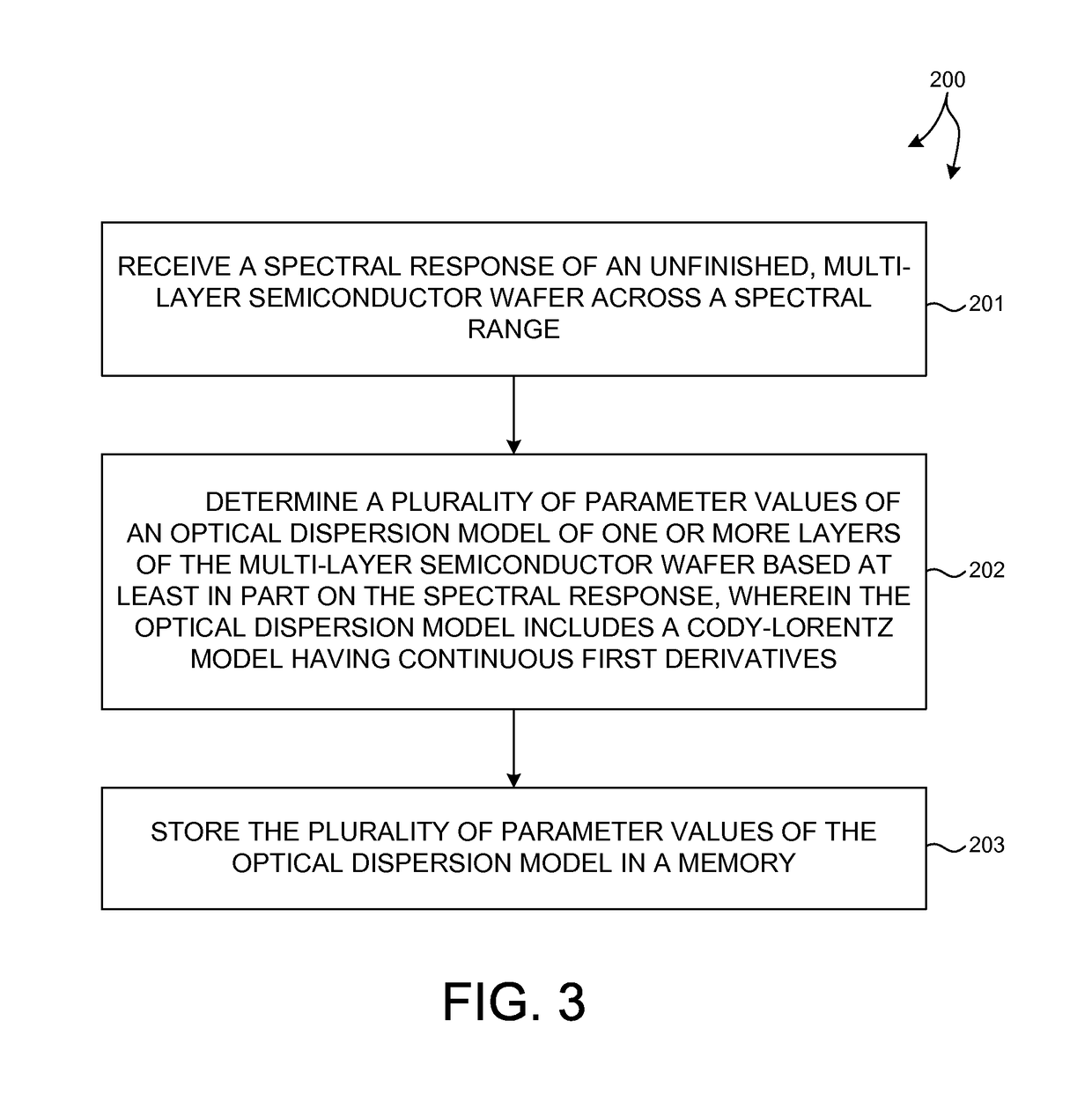
[0029]Optical models of semiconductor structures such as gate dielectric stacks are presented. In particular, models capable of accurate characterization of band structure characteristics in high-K dielectric layers and nanostructures based on high-K dielectric materials are presented. These models quickly and accurately represent experimental results in a physically meaningful manner that can be subsequently used to gain insight and control over a manufacturing process.

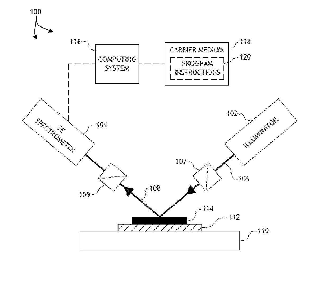
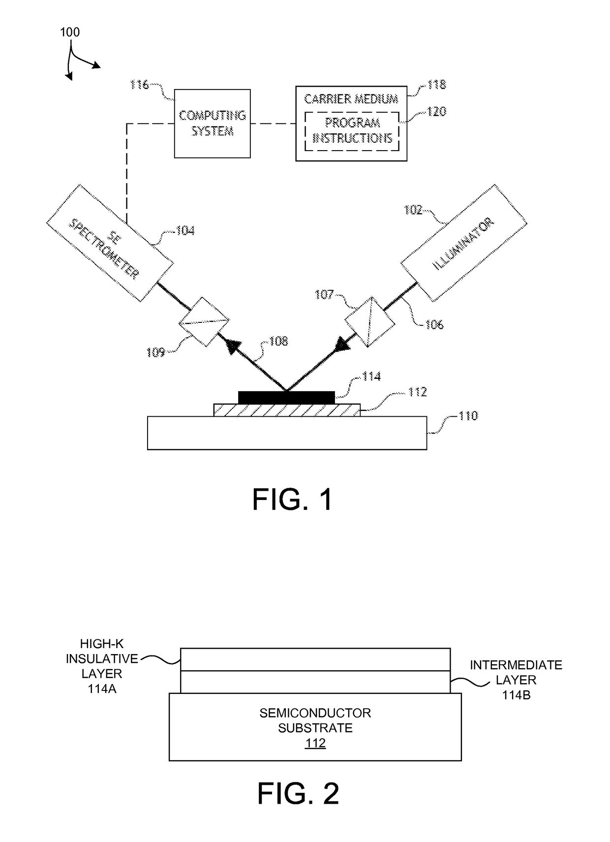
[0030]FIG. 1 illustrates a system 100 for measuring a spectral response of a thin film of a semiconductor wafer, in accordance with one embodiment of the present invention. As shown in FIG. 1, the system 100 may be used to perform spectroscopic ellipsometry on one or more films 114 of a semiconductor wafer 112 disposed on a translation stage 110. In th...


PUM

PropertyMeasurementUnit
wavelength rangeaaaaaaaaaa
optical dispersion modelaaaaaaaaaa
dielectric functionaaaaaaaaaa

Abstract

Methods and systems for determining band structure characteristics of high-k dielectric films deposited over a substrate based on spectral response data are presented. High throughput spectrometers are utilized to quickly measure semiconductor wafers early in the manufacturing process. Optical models of semiconductor structures capable of accurate characterization of defects in high-K dielectric layers and embedded nanostructures are presented. In one example, the optical dispersion model includes a continuous Cody-Lorentz model having continuous first derivatives that is sensitive to a band gap of a layer of the unfinished, multi-layer semiconductor wafer. These models quickly and accurately represent experimental results in a physically meaningful manner. The model parameter values can be subsequently used to gain insight and control over a manufacturing process.

Description

CROSS REFERENCE TO RELATED APPLICATION[0001]The present application for patent claims priority under 35 U.S.C. §119 from U.S. provisional patent application Ser. No. 61 / 869,493, entitled “Dispersion Model For Band Gap Tracking,” filed Aug. 23, 2013, the subject matter of which is incorporated herein by reference.TECHNICAL FIELD[0002]The described embodiments relate to systems for wafer inspection, and more particularly to characterization of thin films used in semiconductor manufacturing.BACKGROUND INFORMATION[0003]Semiconductor devices such as logic and memory devices are typically fabricated by a sequence of processing steps applied to a substrate or wafer. The various features and multiple structural levels of the semiconductor devices are formed by these processing steps. For example, lithography among others is one semiconductor fabrication process that involves generating a pattern on a semiconductor wafer. Additional examples of semiconductor fabrication processes include, bu...

Claims


Application Information

Patent Timeline
Patent Type & Authority Patents(United States)
IPC IPC(8): H01L21/66G01R31/26G01N21/95
CPCH01L22/12G01R31/2601G01N21/9501G01N21/211G01N21/8422G01N2021/8438G01N2021/95676G01R31/2648G01N21/27G01R31/2831G01R31/308
Inventor MALKOVA, NATALIAPOSLAVSKY, LEONIDDI, MINGZHAO, QIANGHU, DAWEI
Owner KLA TENCOR TECH CORP
Why Eureka
Try Eureka