On-chip photonic-phononic emitter-receiver apparatus

a phononic emitter and receiver technology, applied in the field of radiofrequency photonic devices, can solve the problems of low signal distortion, elusive optical wavelength insensitivity, and narrow-band rf filter that simultaneously achieves high optical power handling, and achieves strong photon-phonon coupling

Active Publication Date: 2017-07-04
NAT TECH & ENG SOLUTIONS OF SANDIA LLC
View PDF5 Cites 31 Cited by
  • Summary
  • Abstract
  • Description
  • Claims
  • Application Information

AI Technical Summary

Benefits of technology

[0009]We have developed a chip-scale photonic-phononic emitter-receiver (PPER) system that produces strong photon-phonon coupling without req...

Problems solved by technology

Although resonant systems can achieve strong coupling and high frequency selectivity, they also suffer from disadvantages such as sensitivity to the optical wavelength.
Howev...

Method used


Image

  • On-chip photonic-phononic emitter-receiver apparatus
  • On-chip photonic-phononic emitter-receiver apparatus
  • On-chip photonic-phononic emitter-receiver apparatus

Examples


example 1

Phonon Emitter-Receiver

[0098]PPER platforms were fabricated as described above. In an example, the dimensions were:

a0=1 μm

b0=950 nm

c0=220 nm

r0=0.385 μm

t0=130 nm

W0=5.7 μm

N=6

Nc=6

Interaction length=7 mm.

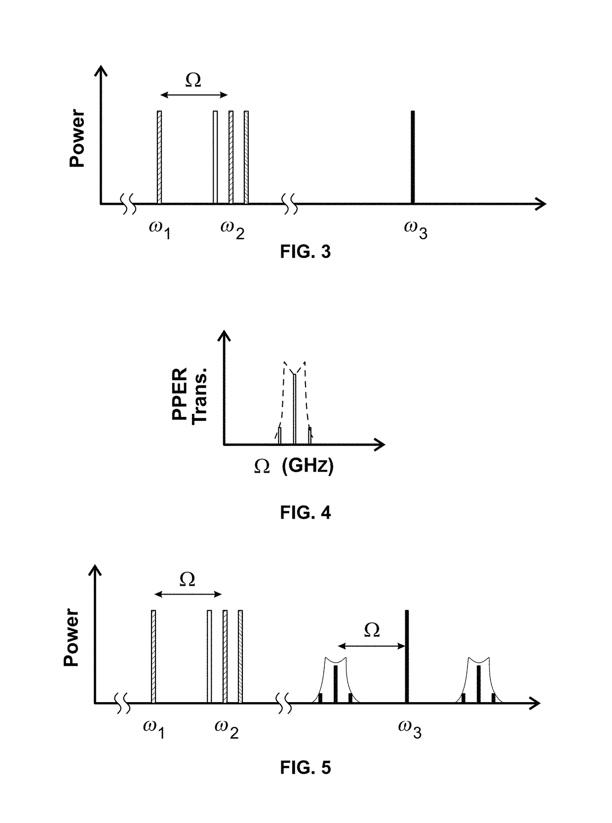
[0099]A single-wavelength laser line at 1547 nm was intensity-modulated, using a Mach-Zehnder modulator, to synthesize pump waves E1a(ω1) and E2a(ω2) (equivalently, a pump wave and a local oscillator wave, as described above) for injection into Wg-A. The carrier-frequency component was suppressed by optimizing the bias voltage, so that only the two sidebands were injected into the waveguide.

[0100]Optical forces, generated through wave interference in Wg-A, drove phonon-mediated coherent information transduction in Wg-B through excitation of hybridized phonon supermodes. The phonon supermodes generated the new signal field Esb(ωs) through travelling-wave phase modulation of the probe wave E3b(ω3), which was injected into Wg-B at a wavelength of 1536 nm. The beat signal between the interf...

example 2

Superdome Engineering

[0109]As explained above, the PPER response is determined solely by phonon supermodes straddling both waveguides. These supermodes are controllable by engineering the PnC structure. For example, the center frequencies of PPER supermodes can be tailored by engineering the defect size Wo.

[0110]FIG. 19 provides two plots of the measured and normalized RF response, i.e. the emit-receive response, of a PPER system as a function of frequency. The two plots compare the effect of changing the defect size Wo. In both plots, the PnC design had N=Nc=6. The left-hand plot had Wo=5.7 μm, and the right-hand plot had Wo=5.2 μm.

[0111]It will be seen that although the lineshape did not change significantly, the center frequency shifted by 250 MHz as the defect size was lithographically varied from 5.7 μm to 5.2 μm.

[0112]The PPER transfer function can also be shaped by lithographically controlling N, Nc and Wo to control the frequency splitting and decay rate of the PnC supermode...


PUM


Abstract

A radio-frequency photonic devices employs photon-phonon coupling for information transfer. The device includes a membrane in which a two-dimensionally periodic phononic crystal (PnC) structure is patterned. The device also includes at least a first optical waveguide embedded in the membrane. At least a first line-defect region interrupts the PnC structure. The first optical waveguide is embedded within the line-defect region.

Description

STATEMENT OF GOVERNMENT INTEREST[0001]This invention was made with Government support under Contract No. DE-AC04-94AL85000 awarded by the U.S. Department of Energy. The Government has certain rights in the invention.FIELD OF THE INVENTION[0002]The invention relates to radio-frequency photonic devices, and more particularly to devices that employ photon-phonon coupling for information transfer.ART BACKGROUND[0003]Interactions between photons and phonons in engineerable micro-scale and nano-scale structures and materials have attracted interest for the purpose of chip-scale radiofrequency (RF) photonic signal processing.[0004]For example, U.S. Pat. No. 8,600,200 by P. T. Rakich et al., assigned at least in part to an assignee hereof, issued on Dec. 3, 2013 under the title “Nano-Optomechanical Transducer,” describes a nano-optomechanical transducer in which transmitting and receiving optical waveguides are mechanically coupled to a suspended membrane. An input optical signal generates ...

Claims


Application Information

Patent Timeline
IPC IPC(8): G02F1/295G02B1/00G02F1/125G02B6/122G02B6/12
CPCG02B6/1225G02F1/125G02B1/005G02B2006/12061G02F2/002G02F2/004G02F2202/32H04B1/40
Inventor COX, JONATHAN ALBERTJARECKI, JR., ROBERT L.RAKICH, PETER THOMASWANG, ZHENGSHIN, HEEDEUKSIDDIQUI, ALEEMSTARBUCK, ANDREW LEA
Owner NAT TECH & ENG SOLUTIONS OF SANDIA LLC
Why Eureka
Try Eureka