Method for manufacture of fine line circuitry

a technology of fine line circuitry and manufacturing method, which is applied in the direction of printed element electric connection formation, insulating substrate metal adhesion improvement, liquid/solution decomposition chemical coating, etc., can solve the problems of undesired delamination of copper, weak adhesion between the conductive layer and the dielectric surface of the build-up layer, and undesired delamination of the copper layer. , to achieve the effect of avoiding or minimizing the disadvantages

Active Publication Date: 2017-07-18
ATOTECH DEUT GMBH
View PDF19 Cites 3 Cited by
  • Summary
  • Abstract
  • Description
  • Claims
  • Application Information

AI Technical Summary

Benefits of technology

[0011]Therefore, it is the objective of the present invention to provide a method for manufacture of fine line circuitry which avoids or minimizes the disadvantages derived from the roughening of the top surface of the build-up layer (1) prior to deposition of a conductive layer onto said roughened top surface while providing a sufficient adhesion between the conductive layer (6) and the top surface of the build-up layer (1).SUMMARY OF THE INVENTION
[0022]The first conductive layer (10) shows a sufficient adhesion to the front side (1a) surface area of the build-up layer (1). Furthermore, because no desmear process is applied to the front side (1a) surface area of the build-up layer (1) prior to deposition of the first conductive layer (10) and because the first conductive layer (10) also serves as a protection layer when cleaning the side walls and the copper area (2) of the at least one opening (4), a smooth front side (1a) surface area of the build-up layer (1) is maintained and hence, formation of fine line circuitry such as one having a line width and inter line spacing of 10 μm or less is possible. The smooth front side (1a) surface area of the build-up layer (1) also enables to use mild etching conditions in order to completely remove in step (ix) those portions of the first conductive layer (10) which were covered by the patterned resist layer (7) in steps (vi) and (vii).
[0023]Accordingly, the desired shape of electroplated copper features can be achieved and a high adhesion between the first conductive layer (10) and the front side (1a) surface area of the build-up layer (1) is maintained after cleaning the side walls and the copper area (2) of the at least one opening (4).

Problems solved by technology

One disadvantage of the SAP method is the weak adhesion between the conductive layer (6) and the dielectric surface of the build-up layer (1).
The weak adhesion can lead to an undesired delamination of the copper tracks formed by subsequent electroplating of copper onto the conductive layer (6) in later manufacturing steps or later use of the printed circuit board.
On the one hand, roughening of the dielectric surface is necessary to provide adhesion between the dielectric surface and the conductive layer (6), on the other hand a roughened top surface (5a) of the build-up layer (1) does not allow formation of a fine line circuitry such as one having a line width and inter line spacing of 10 μm or less.
Severe etch conditions lead to an undesired attack of the copper layer (8) and the desired shape of electroplated copper features can not be achieved.

Method used


Image

  • Method for manufacture of fine line circuitry
  • Method for manufacture of fine line circuitry
  • Method for manufacture of fine line circuitry

Examples


Embodiment Construction

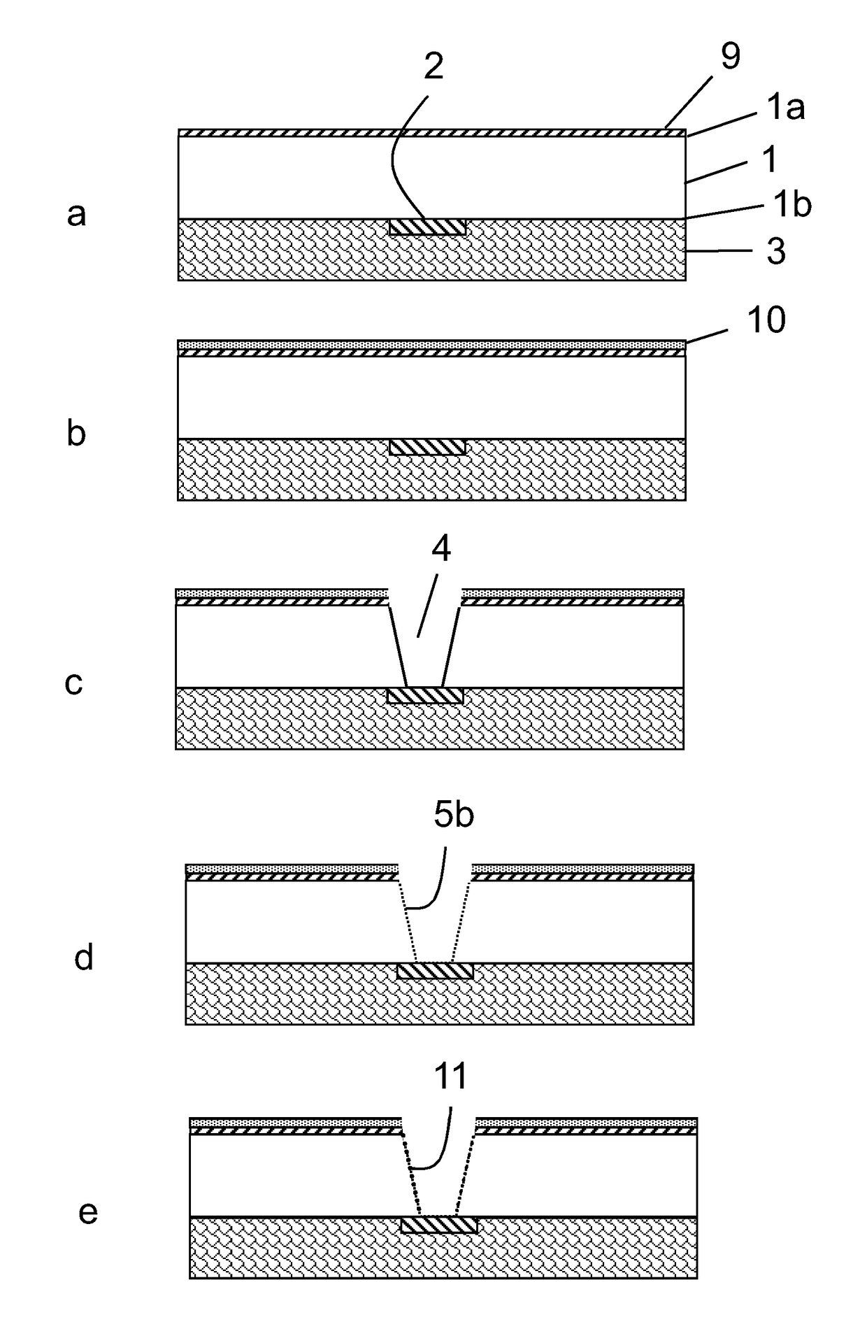
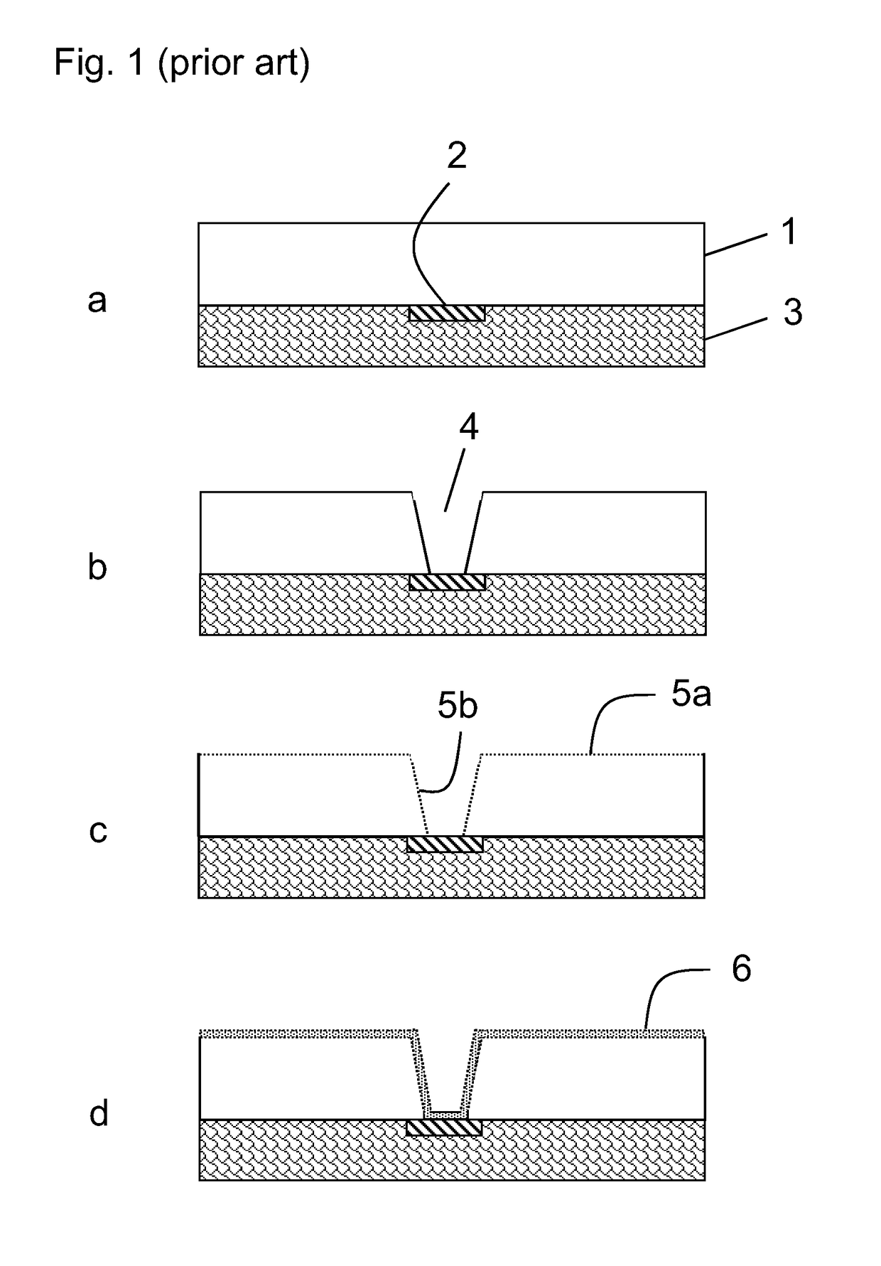
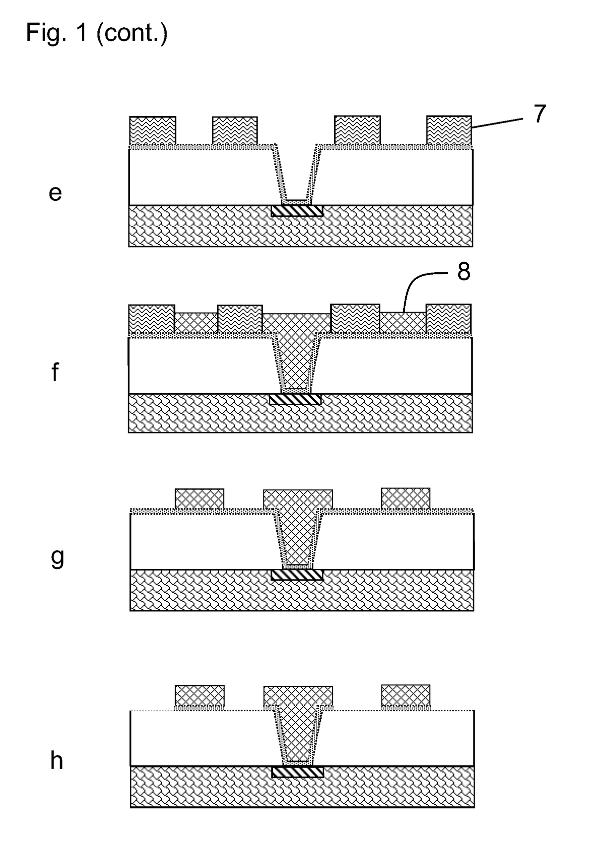
[0026]The method for manufacture of fine line circuitry is in more detail described below. The figures shown herein are simply illustrative of the process. The figures are not drawn to scale, i.e. they do not reflect the actual dimensions or features of the various layers in the laminate. Like numbers refer to like elements throughout the description.

[0027]Now referring to FIG. 2a, in accordance with a preferred embodiment of the present invention, there is provided a dielectric build-up layer (1) which may be made of an organic material or a fiber-reinforced organic material or a particle-reinforced organic material, etc., for example, epoxy resin, polyimide, bismaleimide triazine, cyanate ester, polybenzocyclobutene, or glass fiber composite thereof, etc. The build-up layer (1) comprises a front side (1a) and a back side (1b). The front side (1a) of the build-up layer (1) consists of bare dielectric material having a smooth surface which comprises an adhesion promoting layer (9). ...


PUM

PropertyMeasurementUnit
thicknessaaaaaaaaaa
widthaaaaaaaaaa
temperatureaaaaaaaaaa

Abstract

The present invention relates to a method for manufacture of fine line circuitry in the manufacture of printed circuit boards, IC substrates and the like. The method utilizes a first conductive layer on the smooth surface of a build-up layer and a second conductive layer selected from electrically conductive polymers, colloidal noble metals and electrically conductive carbon particles on the roughened walls of at least one opening which are formed after depositing the first conductive layer.

Description

[0001]The present application is a U.S. National Stage Application based on and claiming benefit and priority under 35 U.S.C. §371 of International Application No. PCT / EP2013 / 052318, filed 06 Feb. 2013, which in turn claims benefit of and priority to European Application No. 12075035.1, filed 29 Mar. 2012, the entirety of each of which is hereby incorporated herein by reference.FIELD OF THE INVENTION[0002]The present invention relates to a method for manufacture of printed circuit boards, IC substrates and the like. More particularly, the invention relates to a method for manufacture of fine line circuitry.BACKGROUND OF THE INVENTION[0003]The ongoing miniaturization of features of HDI printed circuit boards, IC substrates and the like requires more advanced manufacturing methods than conventional methods such as formation of circuitry by a print and etch method.[0004]A method for manufacture of fine line circuitry known in the art is the semi-additive process (SAP) which starts from...

Claims


Application Information

Patent Timeline
Patent Type & Authority Patents(United States)
IPC IPC(8): C25D5/56H05K3/46C23C18/40C25D7/06C25D7/00H05K3/06H05K3/38C23C18/16C23C18/20H05K3/42C25D5/02H05K3/10C23C18/30C25D3/38
CPCH05K3/387C23C18/1653C23C18/2006C23C18/40C25D5/022C25D5/56C25D7/00C25D7/06H05K3/06H05K3/381H05K3/389H05K3/421H05K3/4644C23C18/2066C23C18/30C23C18/405C25D3/38H05K3/108H05K3/388H05K2203/0789H05K2203/0793H05K2203/0796
Inventor NICHOLS, RICHARDJANG, DONRIEBEL, HARALDBRUNING, FRANK
Owner ATOTECH DEUT GMBH
Why Eureka
Try Eureka