Method for epitaxial growth of monocrystalline silicon carbide using a feed material including a surface layer containing a polycrystalline silicon carbide with a 3C crystal polymorph

a polymorphic silicon carbide and epitaxial growth technology, which is applied in the field of monocrystalline silicon carbide epitaxial growth feed material, can solve the problems of difficult control of the epitaxial growth process of silicon carbide, high cost of silicon carbide epitaxial growth film production, so as to increase the epitaxial growth rate of monocrystalline silicon carbide

Inactive Publication Date: 2017-08-08
TOYO TANSO KK
View PDF14 Cites 1 Cited by
  • Summary
  • Abstract
  • Description
  • Claims
  • Application Information

AI Technical Summary

Benefits of technology

[0053]The present invention can provide a feed material for epitaxial growth of a monocrystalline silicon carbide capable of increasing the rate of epitaxial growth of a monocrystalline silicon carbide.

Problems solved by technology

Therefore, in the case of using the modified Lely method, a large apparatus is required for epitaxial growth of silicon carbide and the process for epitaxial growth of silicon carbide is difficult to control.
This presents a problem of rise in cost of producing a silicon carbide epitaxial growth film.
Therefore, crystal defects are likely to occur in the silicon carbide epitaxial growth film being formed and there also arises a problem of ease of roughening of the crystal structure.

Method used


Image

  • Method for epitaxial growth of monocrystalline silicon carbide using a feed material including a surface layer containing a polycrystalline silicon carbide with a 3C crystal polymorph
  • Method for epitaxial growth of monocrystalline silicon carbide using a feed material including a surface layer containing a polycrystalline silicon carbide with a 3C crystal polymorph
  • Method for epitaxial growth of monocrystalline silicon carbide using a feed material including a surface layer containing a polycrystalline silicon carbide with a 3C crystal polymorph

Examples


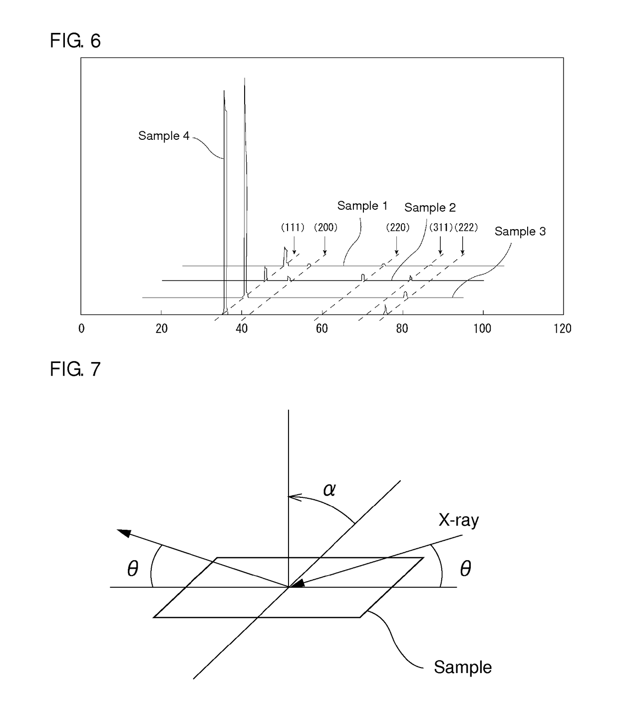
production example 1

[0107]A graphite material (15 mm by 15 mm by 2 mm) made of high-purity isotropic graphite having a bulk density of 1.85 g / cm3 and an ash content of 5 ppm or less was used as a base material. The base material was put into a CVD reactor and a 30 μm thick polycrystalline silicon carbide coating was formed on the base material by CVD to produce Sample 1. Silicon tetrachloride and propane gas were used as source gases. The deposition was performed at an ordinary pressure and 1200° C. The deposition rate was at 30 μm / h.

production example 2

[0108]A 50 μm thick polycrystalline silicon carbide coating was formed on the surface of a graphite material in the same manner as in Production Example 1 above except that the reaction temperature was at 1400° C. and the deposition rate was at 60 μm / h, resulting in the production of Sample 2.

production example 3

[0109]A 50 μm thick polycrystalline silicon carbide coating was formed on the surface of a graphite material in the same manner as in Production Example 1 above except that the reaction temperature was at 1250° C., the deposition rate was at 10 μm / h, and CH3SiCl3 was used instead of silicon tetrachloride, resulting in the production of Sample 3.


PUM

PropertyMeasurementUnit
orientation angleaaaaaaaaaa
thicknessaaaaaaaaaa
temperatureaaaaaaaaaa

Abstract

Provided is a feed material for epitaxial growth of a monocrystalline silicon carbide capable of increasing the rate of epitaxial growth of silicon carbide. A feed material 11 for epitaxial growth of a monocrystalline silicon carbide includes a surface layer containing a polycrystalline silicon carbide with a 3C crystal polymorph. Upon X-ray diffraction of the surface layer, a diffraction peak corresponding to a (111) crystal plane and a diffraction peak other than the diffraction peak corresponding to the (111) crystal plane are observed as diffraction peaks corresponding to the polycrystalline silicon carbide with a 3C crystal polymorph.

Description

TECHNICAL FIELD[0001]This invention relates to a feed material for epitaxial growth of a monocrystalline silicon carbide and a method for epitaxial growth of a monocrystalline silicon carbide using the same.BACKGROUND ART[0002]Silicon carbide (SiC) is considered to be capable of achieving high-temperature resistance, high voltage resistance, high-frequency resistance, and high environment resistance each of which could not be achieved by conventional semiconductor materials, such as silicon (Si) and gallium arsenide (GaAs). Therefore, silicon carbide is expected as a semiconductor material for next-generation power devices and a semiconductor material for high-frequency devices.[0003]The seeded sublimation growth method (modified Lely method) is conventionally proposed as a method for growing a monocrystalline silicon carbide, such as for example in Patent Literature 1 below. In this modified Lely method, a seed material made of a monocrystalline silicon carbide is placed in a low-t...

Claims


Application Information

Patent Timeline
Patent Type & Authority Patents(United States)
IPC IPC(8): C30B19/12C30B19/00C30B28/12C30B29/36
CPCC30B19/12C30B19/00C30B28/12C30B29/36Y10T428/26
Inventor TORIMI, SATOSHINOGAMI, SATORUMATSUMOTO, TSUYOSHI
Owner TOYO TANSO KK
Why Eureka
Try Eureka