Method of fabricating wafer

a technology of fabricating and wafers, applied in the direction of chemically reactive gases, crystal growth processes, after-treatment details, etc., can solve the problems of generating large leakage current, presenting various defects, and affecting the performance of the semiconductor device employing the wafer, so as to prevent defects, and reduce the risk of contamination

Active Publication Date: 2017-08-29
LX SEMICON CO LTD
View PDF10 Cites 0 Cited by
  • Summary
  • Abstract
  • Description
  • Claims
  • Application Information

AI Technical Summary

Benefits of technology

[0009]The method of fabricating the wafer according to the embodiment comprises the stepwise cooling. Through the stepwise cooling, the strain caused by thermal stress generated when the wafer is grown can be attenuated. Thus, the defects can be prevented and the performance of the wafer can be improved by controlling the defects. In addition, the embodiment can provide the wafer having high quality by controlling the warping and twisting of the epitaxial wafer.
[0010]According to the embodiment, a buffer layer can be removed without the defect, so the process can be simplified. In addition, an additional process to form the buffer layer can be omitted so that the fabrication cost can be reduced and the quality of the substrate surface can be improved.
[0011]The method of fabricating the wafer according to another embodiment comprises the annealing step. By performing the annealing step, the mismatch between the wafer and the wafer caused by the thermal expansion can be suppressed.

Problems solved by technology

For instance, there may be presented various defects, such as a defect created in a basal plane of a lattice, a defect caused by the tilting of the lattice, and a defect created on a surface of the wafer.
These defects may exert bad influence upon the semiconductor device employing the wafer.
In addition, when the semiconductor device is fabricated by using the wafer, great leakage current may be generated due to the non-uniformity of metal electrode deposition and patterns.
Due to the above additional processes, the fabrication process is complicated, the fabrication cost is increased, and the quality of a substrate surface is deteriorated.

Method used


Image

  • Method of fabricating wafer
  • Method of fabricating wafer
  • Method of fabricating wafer

Examples


first embodiment

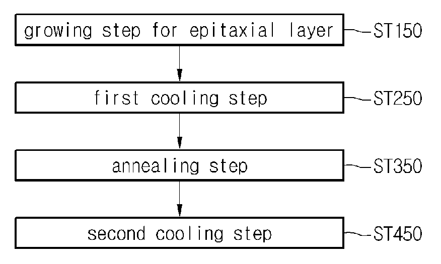
[0028]Referring to FIGS. 1 and 2, the method of fabricating the wafer comprises a growing step ST100 for an wafer and a cooling step ST200.

[0029]In growing step ST100 for the wafer, the wafer may be grown on the surface of the wafer. The wafer can be formed by growing a single crystal layer including a material equal to or different from a material for the wafer on the surface of a single crystal wafer.

[0030]In general, the wafer can be formed through a chemical vapor deposition (CVD) process. Especially, the CVD process may comprise thermal CVD, plasma enhanced CVD, low-pressure CVD, metal organic CVD, and atomic layer deposition processes. These processes may be properly selected according to the characteristic of the target layer to be formed.

[0031]In the case of the CVD process, reaction gas, such as source gas, carrier gas or pressure adjusting gas, is supplied onto the wafer placed in a vacuum chamber and the wafer is formed on the wafer through the surface reaction between t...

second embodiment

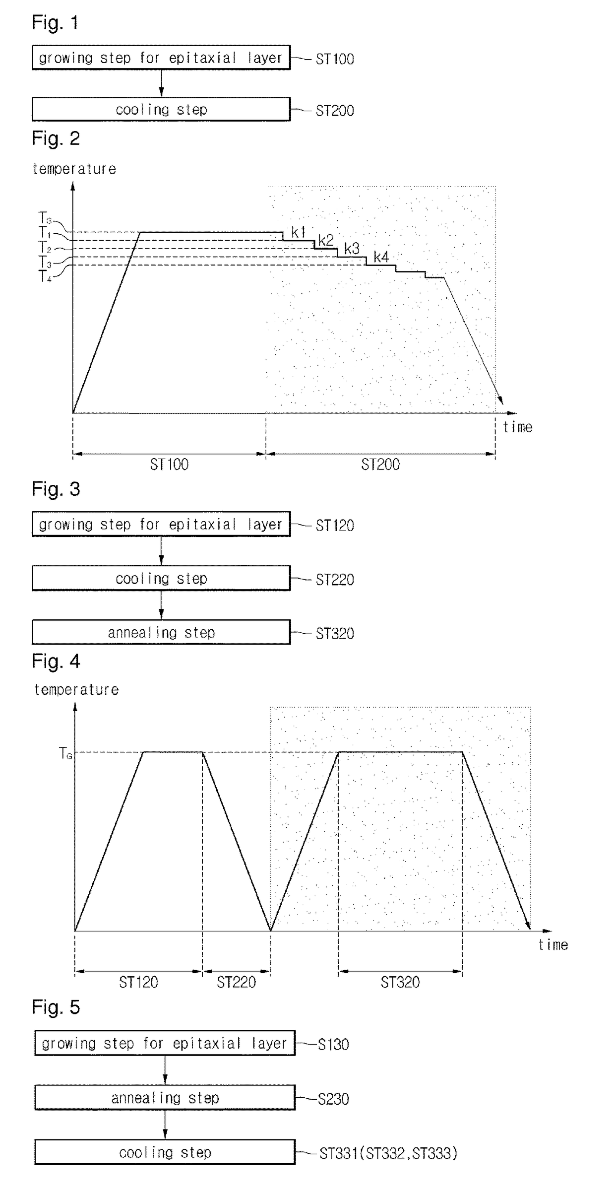
[0052]Referring to FIGS. 3 and 4, the method of fabricating the wafer comprises a growing step ST120 for an wafer, a cooling step ST220 and an annealing step ST320.

[0053]In growing step ST120 for the wafer, the wafer may be grown on the surface of the wafer.

[0054]In growing step ST120 for the wafer, the wafer can be grown in a first chamber under the predetermined growth temperature TG. For instance, the growth temperature TG is in the range of 1300° C. to 1700° C.

[0055]After the wafer has been grown, the wafer is subject to cooling step ST220. In cooling step ST220, the growth temperature TG is lowered to stabilize the wafer on the wafer.

[0056]However, in cooling step ST220, the cooling rate in the wafer may not be uniform. That is, the cooling rate at the center of the wafer may be lower than the cooling rate at the outer peripheral portion of the wafer. Thus, the temperature may be slowly dropped at the center of the wafer relative to the outer peripheral portion of the wafer. I...

third embodiment

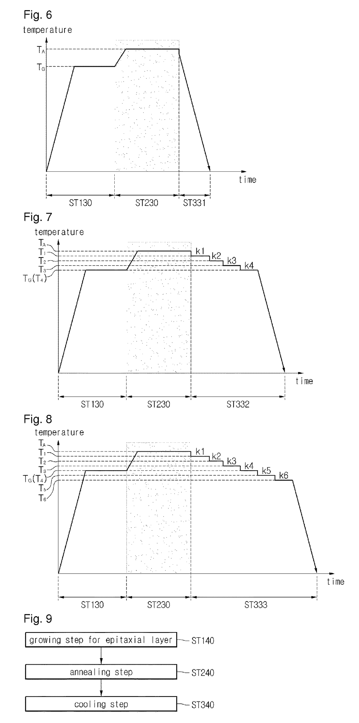
[0065]Referring to FIGS. 5 and 6, the method of fabricating the wafer comprises a growing step ST130 for an wafer, an annealing step ST230 and a cooling step ST331.

[0066]In growing step ST130 for the wafer, the wafer may be grown on the surface of the wafer.

[0067]Then, the epitaxial wafer is annealed in annealing step ST230. That is, the epitaxial wafer is heat-treated at a predetermined temperature.

[0068]Annealing step ST230 can be performed at the temperature TA higher than the growth temperature TG. In detail, the annealing temperature TA may be higher than the growth temperature TG by 100° C. to 200° C. In addition, annealing step ST230 can be performed for about 1 hour.

[0069]Annealing step ST230 can be performed under the high vacuum condition.

[0070]Annealing step ST230 can be performed in a chamber where growing step ST130 for the wafer is performed. That is, annealing step ST230 can be performed in-situ so the process time can be reduced.

[0071]The mismatch between the wafer ...


PUM

PropertyMeasurementUnit
angleaaaaaaaaaa
angleaaaaaaaaaa
temperatureaaaaaaaaaa

Abstract

A method of fabricating a wafer according to the embodiment comprises the steps of growing an wafer on a surface of the wafer in a growth temperature; and cooling the wafer after the wafer has been grown, wherein a stepwise cooling is performed when cooling the wafer.

Description

CROSS-REFERENCE TO RELATED APPLICATIONS[0001]This application is the U.S. national stage application of International Patent Application No. PCT / KR2012 / 004963, filed Jun. 22, 2012, which claims priority to Korean Applications Nos. 10-2011-0060906, filed Jun. 22, 2011, 10-2011-0060907, filed Jun. 22, 2011, 10-2011-0060910, filed Jun. 22, 2011, 10-2011-0060912, filed Jun. 22, 2011, and 10-0060913, filed Jun. 22, 2011, the disclosures of each of which are incorporated herein by reference in their entirety.TECHNICAL FIELD[0002]The disclosure relates to a method of fabricating a wafer.BACKGROUND ART[0003]The most important subject in studies for improving the efficiency and characteristic of semiconductor devices is to reduce the crystal defect of a semiconductor layer grown on a substrate and to improve crystallinity of the semiconductor layer.[0004]Various types of defects may be formed when fabricating an epitaxial wafer (hereinafter, these defects will be referred to as epitaxial def...

Claims


Application Information

Patent Timeline
Patent Type & Authority Patents(United States)
IPC IPC(8): C30B1/02C30B25/16H01L21/02C23C16/46C30B33/00H01L21/324C30B33/02
CPCC30B25/16C23C16/463C30B33/00C30B33/02H01L21/0262H01L21/02378H01L21/02433H01L21/02532H01L21/02664H01L21/324
Inventor KANG, SEOK MINKIM, MOO SEONG
Owner LX SEMICON CO LTD
Why Eureka
Try Eureka