Vacuum-integrated hardmask processes and apparatus

a vacuum-integrated, hard-mask technology, applied in the field of vacuum-integrated hard-mask processes and apparatuses, can solve the problems of loss of resolution, affecting the performance of euv lithography, observing line edge roughness (ler) and linewidth variation of patterned resist, etc., to achieve the effect of improving euv lithography (euvl) performance and reducing line edge roughness

Active Publication Date: 2017-10-03
LAM RES CORP
View PDF29 Cites 177 Cited by
  • Summary
  • Abstract
  • Description
  • Claims
  • Application Information

AI Technical Summary

Benefits of technology

[0006]In one implementation, a EUV-sensitive metal-containing film is deposited on a semiconductor substrate. The metal-containing film is then patterned directly by EUV exposure in a vacuum ambient to form the metal hardmask. In this way, a vacuum-integrated metal hardmask process and related vacuum-integrated hardware that combine steps of film

Problems solved by technology

This unwanted secondary electron exposure results in loss of resolution, observable line edge roughness (LER) and linewidth variation in the patterned res

Method used


Image

  • Vacuum-integrated hardmask processes and apparatus
  • Vacuum-integrated hardmask processes and apparatus
  • Vacuum-integrated hardmask processes and apparatus

Examples


Embodiment Construction

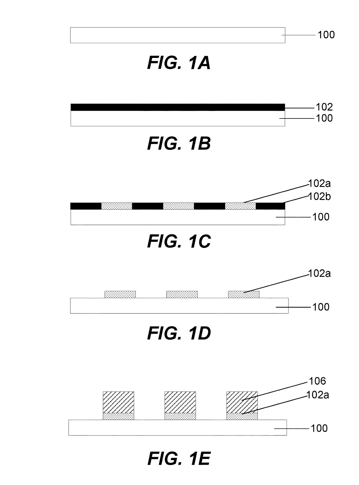
[0012]Reference will now be made in detail to specific embodiments of the invention. Examples of the specific embodiments are illustrated in the accompanying drawings. While the invention will be described in conjunction with these specific embodiments, it will be understood that it is not intended to limit the invention to such specific embodiments. On the contrary, it is intended to cover alternatives, modifications, and equivalents as may be included within the spirit and scope of the invention. In the following description, numerous specific details are set forth in order to provide a thorough understanding of the present invention. The present invention may be practiced without some or all of these specific details. In other instances, well known process operations have not been described in detail so as to not unnecessarily obscure the present invention.

INTRODUCTION

[0013]Extreme ultraviolet (EUV) lithography can extend lithographic technology beyond its optical limits by movin...


PUM

PropertyMeasurementUnit
Thicknessaaaaaaaaaa
Pressureaaaaaaaaaa
Wavelengthaaaaaaaaaa

Abstract

Vacuum-integrated photoresist-less methods and apparatuses for forming metal hardmasks can provide sub-30 nm patterning resolution. A metal-containing (e.g., metal salt or organometallic compound) film that is sensitive to a patterning agent is deposited on a semiconductor substrate. The metal-containing film is then patterned directly (i.e., without the use of a photoresist) by exposure to the patterning agent in a vacuum ambient to form the metal mask. For example, the metal-containing film is photosensitive and the patterning is conducted using sub-30 nm wavelength optical lithography, such as EUV lithography.

Description

CROSS-REFERENCE TO RELATED APPLICATIONS[0001]This application claims priority to U.S. Provisional Patent Application No. 61 / 934,514 filed Jan. 31, 2014, titled VACUUM-INTEGRATED HARDMASK PROCESSES, which is incorporated herein by reference in its entirety and for all purposes.BACKGROUND[0002]This disclosure relates generally to the field of semiconductor processing. In particular, the disclosure is directed to vacuum-integrated processes for forming metal hardmasks without the use of photoresist.[0003]Patterning of thin films in semiconductor processing is often a critical step in the manufacture and fabrication of semiconductors. Patterning involves lithography. In conventional photolithography, such as 193 nm photolithography, patterns are printed by emitting photons from a photon source onto a mask and printing the pattern onto a photosensitive photoresist, thereby causing a chemical reaction in the photoresist that, after development, removes certain portions of the photoresist ...

Claims


Application Information

Patent Timeline
IPC IPC(8): B05D3/06C23C18/16C23C18/18H01L21/033H01L21/3213C23C18/14G03F1/76G03F7/004G03F7/16
CPCG03F1/76C23C18/14C23C18/165C23C18/1612C23C18/182G03F7/0043G03F7/16G03F7/167H01L21/0332H01L21/0337H01L21/3213C23C18/143C23C18/145H01L21/31144H01L21/32139H01L21/67161H01L21/3086H01L29/66795C23C14/56G03F7/70808G03F7/26G03F7/36H01L21/67167H01L21/67213C23C16/44
Inventor MARKS, JEFFREYANTONELLI, GEORGE ANDREWGOTTSCHO, RICHARD A.HAUSMANN, DENNIS M.LAVOIE, ADRIENKNISLEY, THOMAS JOSEPHREDDY, SIRISH K.VARADARAJAN, BHADRI N.KOLICS, ARTUR
Owner LAM RES CORP
Why Eureka
Try Eureka