Supercharge Your Innovation With Domain-Expert AI Agents!

Electro-optical modulator

a modulator and waveguide technology, applied in non-linear optics, instruments, optics, etc., can solve the problems of limited modulation speed, low cost of soi substrate, and comparatively slow carrier relaxation time, and achieve the effect of little optical loss

Active Publication Date: 2017-11-28
NAT INST OF ADVANCED IND SCI & TECH +1
View PDF17 Cites 2 Cited by
  • Summary
  • Abstract
  • Description
  • Claims
  • Application Information

AI Technical Summary

Benefits of technology

This configuration allows for high-speed operation with minimal optical loss, leveraging the fast carrier relaxation properties of a-Si:H and enabling modulation speeds beyond 1 Gbps, while maintaining low-temperature fabrication feasibility.

Problems solved by technology

In silicon photonics technology, it is common to use a silicon on insulator (SOI) substrate, in which single crystalline silicon (c-Si) is formed on top of a buried oxide (BOX) film, but there is a problem that an extremely high temperature process of 1100° C. or higher is required to form the c-Si, and the SOI substrate is expensive.
Many electro-optical modulators based on c-Si have been reported on (for example, patent document 1), but in the case of c-Si, one of major factors is that the carrier relaxation time is comparatively slow and the modulation speed is limited.
However, in the case of the electro-optical modulator described in non-patent document 2, it is extremely difficult to obtain a high-speed modulation operation of a nature that exceeds 1 Gbps, because a-SiC:H, which has extremely low mobility and conductivity, is used in the p-type layer (102) and the n-type layer (104).

Method used


Image

  • Electro-optical modulator
  • Electro-optical modulator
  • Electro-optical modulator

Examples


first embodiment

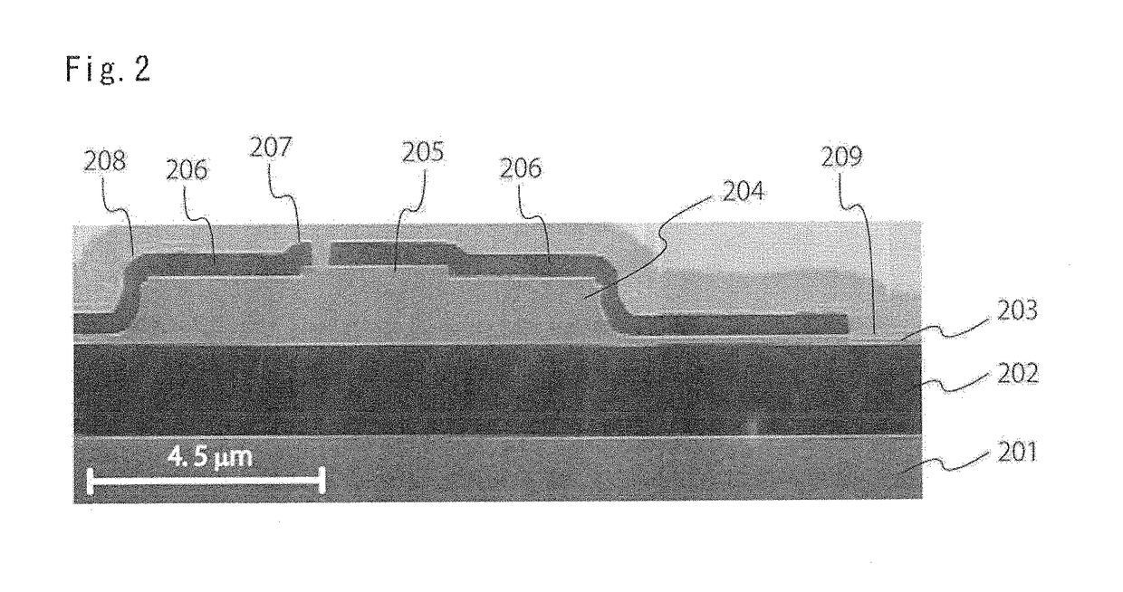
[0053]FIG. 1 is a cross-sectional schematic diagram of a first embodiment of the present invention.

[0054]This electro-optical modulator is provided with a silicon thermal oxide film 202 obtained on a silicon substrate 201 by thermally oxidizing the silicon substrate, and an approximately 0.1 μm-thick B (boron)-doped p-type μc-Si:H layer 203, an approximately 1.3 μm-thick non-doped i-type a-Si:H layer 204, and an approximately 0.1 μm-thick P (phosphorus)-doped n-type μc-Si:H layer 205 are layered in a vertical direction thereon.

[0055]A silicon oxide film 206, an ITO (indium tin oxide) film 207, and electrodes 208 and 209 comprising aluminum (Al) are further provided thereon.

[0056]Because the layers 203, 204, and 205 have approximately the same refractive index (3.4 to 3.6) as each other, and the refractive index is higher than the about 1.44 refractive index of the silicon thermal oxide film 202, silicon oxide film 206, and ITO film 207, the former layers act as an optical waveguide ...

second embodiment

[0085]FIG. 5 is a cross-sectional schematic diagram of a second embodiment of the present invention.

[0086]In the second embodiment, the p-type semiconductor layer and the n-type semiconductor layer are in a vertically stacked arrangement with the optical waveguide comprising an i-type amorphous semiconductor interposed therebetween, and electrode lead-out on the upper layer is made possible.

[0087]The electro-optical modulator illustrated in FIG. 5 is provided with a silicon thermal oxide film 302 obtained on a silicon substrate 301 by thermally oxidizing the silicon substrate, and a vertically stacking of a B (boron)-doped p-type μc-Si:H layer 303, a non-doped i-type a-Si:H layer 304, and a P (phosphorus)-doped n-type μc-Si:H layer 305 are provided thereon.

[0088]A silicon oxide film 306, an indium zinc oxide (IZO) film 307, and an electrode 308 are further provided thereon. An IZO film 309 and an electrode 310 are also provided as lead-out electrodes of the B (boron)-doped p-type μc...

modified example 1

of the Second Embodiment

[0104]FIG. 6 illustrates a modified example 1 of the second embodiment.

[0105]The basic structure of the electro-optical modulator illustrated as modified example 1 in FIG. 6 is approximately the same as that of the second embodiment, but in this modified example 1, the shape of the n-type μs-Si:H layer 305 differs from that in the second embodiment.

[0106]In the structure in FIG. 6, the IZO film 307 having non-negligible optical absorption or the electrode 309 can be moved far from the optical waveguide, and the optical loss of the electro-optical modulator can be reduced.


PUM

PropertyMeasurementUnit
temperatureaaaaaaaaaa
refractive indexaaaaaaaaaa

Abstract

An electro-optical modulator includes a substrate 201; an optical waveguide formed of a silicon-containing i-type amorphous semiconductor 204 on the substrate; and a silicon-containing p-type semiconductor layer 203 and a silicon-containing n-type semiconductor layer 205 arranged apart from each other with the silicon-containing optical waveguide formed of an i-type amorphous semiconductor 204 interposed therebetween and constituting optical waveguides together with the silicon-containing optical waveguide formed of an i-type amorphous semiconductor. The silicon-containing p-type semiconductor layer 203 and / or silicon-containing n-type semiconductor layer 205 area crystalline semiconductor layer.

Description

TECHNICAL FIELD[0001]The present invention relates to a waveguide-type electro-optical modulator in which silicon is used.BACKGROUND ART[0002]Much attention is being given to silicon photonics technology that integrates optical devices and electronic devices at high density in a unified manner on the same silicon substrate. There are great expectations for this technology in applications not only in the field of optical communications, but in optically interconnect of integrated circuits, and R&D is progressing vigorously at present.[0003]In silicon photonics technology, it is common to use a silicon on insulator (SOI) substrate, in which single crystalline silicon (c-Si) is formed on top of a buried oxide (BOX) film, but there is a problem that an extremely high temperature process of 1100° C. or higher is required to form the c-Si, and the SOI substrate is expensive.[0004]Also proposed is a silicon photonics technique that uses hydrogenated amorphous silicon (a-Si:H) films, which ...

Claims


Application Information

Patent Timeline
Patent Type & Authority Patents(United States)
IPC IPC(8): G02F1/035G02F1/025G02F1/015
CPCG02F1/025G02F2202/105G02F2202/103G02F2001/0151G02F1/0151
Inventor KAMEI, TOSHIHIROTAKEI, RYOHEIMORI, MASAHIKOSAKAKIBARA, YOUICHIFUJIKATA, JUNICHI
Owner NAT INST OF ADVANCED IND SCI & TECH
Features
  • R&D
  • Intellectual Property
  • Life Sciences
  • Materials
  • Tech Scout
  • Unparalleled Data Quality
  • Higher Quality Content
  • 60% Fewer Hallucinations
Learn More