

Method to thin down indium phosphide layer
a technology of indium phosphide and thin layer, which is applied in the direction of basic electric elements, electrical apparatus, semiconductor devices, etc., can solve the problems of high energy consumption of fin-fet, relatively small drive current, and short channel
- Summary
- Abstract
- Description
- Claims
- Application Information
AI Technical Summary
Benefits of technology
Problems solved by technology
Method used
Image

Examples
Embodiment Construction
[0015]Reference will now be made in detail to exemplary embodiments of the invention, which are illustrated in the accompanying drawings. Wherever possible, the same reference numbers will be used throughout the drawings to refer to the same or like parts.
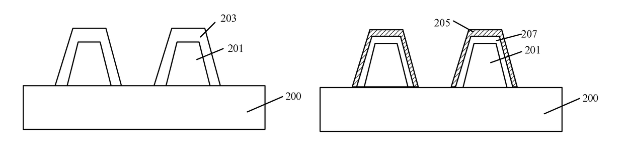
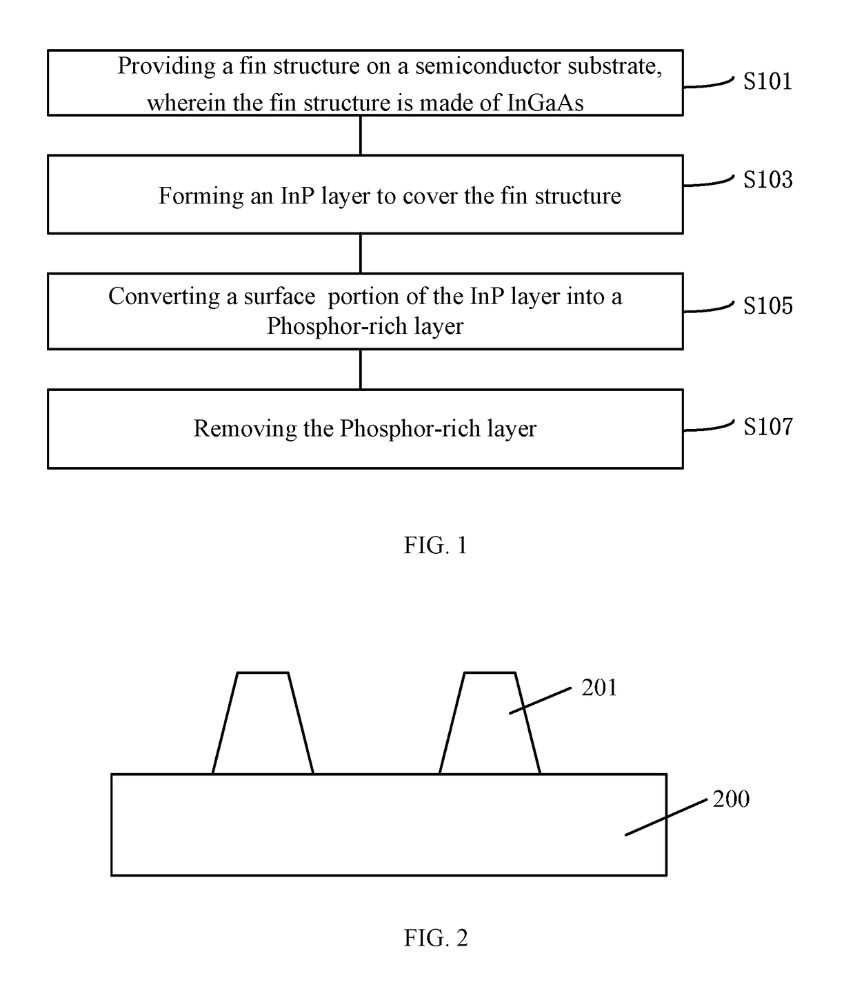
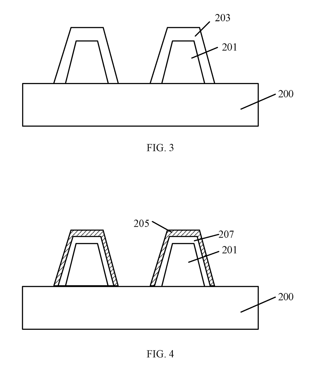
[0016]As described in above background section, existing methods to thin down an InP layer formed on an InGaAs fin structure usually includes performing an ashing process on the InP layer using oxygen gas and then performing a wet etching process at room temperature to remove the ashed portion of the InP layer. During the wet etching process, an etch solution mixed by diluted sulfuric acid and water at a 1:1 ratio may be used. However, the wet etching process may introduce some contaminants, which may affect the performance of the device. In addition, as the device may need to be alternatively handled in dry and wet operation environments, the fabrication process may be more complicated, the processing time may be longer, and the p...
PUM
 Abstract
Description
Claims
Application Information