
Etchant solutions and method of use thereof

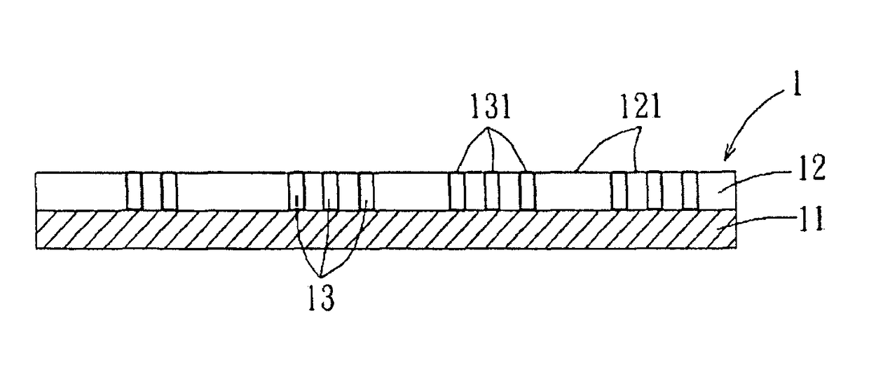
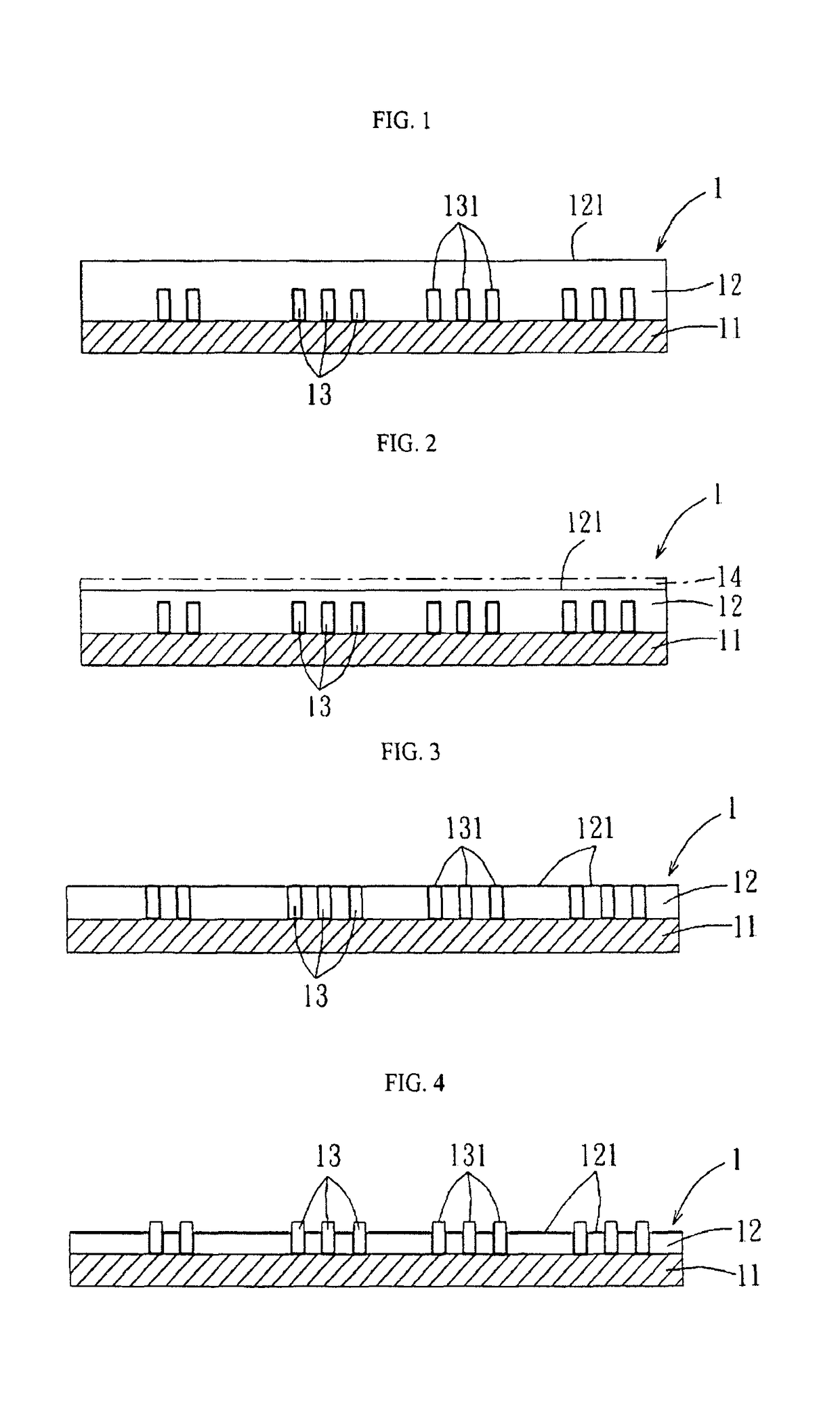
a technology of etchant solution and solution, which is applied in the field of compositions and methods for cleaning microelectronic structures, can solve the problems of adding cost to the device by the tsv process steps, and achieve the effects of low surface roughness, high si etch rate, and low passivation etch

Active Publication Date: 2018-01-23
VERSUM MATERIALS US LLC
View PDF19 Cites 2 Cited by
  • Summary
  • Abstract
  • Description
  • Claims
  • Application Information

AI Technical Summary

Benefits of technology

This patent describes a new etchant composition for silicon that has several advantages over existing methods. It has high rates of silicon etching, low damage to other materials, and smooth surface after cleaning. The composition includes potassium hydroxide and other alkaline compounds. This invention simplifies the etching process and improves the quality of the final product.

Problems solved by technology

TSV process steps add cost to the devices.

Method used


Image

  • Etchant solutions and method of use thereof
  • Etchant solutions and method of use thereof

Examples


working examples

[0042]The following examples are provided for the purpose of further illustrating the present invention but are in no way to be taken as limiting. Unless otherwise noted, all amounts are expressed in weight percent (wt %) based on the total weight of the composition.

[0043]TEST Method to Determine the Si Etch Rate:

[0044]Each etchant composition tested was heated to 70° C. Blank (unpatterned) p-type Si wafer segments 3.5″×5″ in size were cleaved from a whole wafer with exposed [1,0,0] crystal face. The Si segments were pre-treated with buffered oxide etch (BOE) at an ambient temperature of approximately 22° C. for 3 minutes to remove native surface oxide, rinsed in deionized water (DIW) for 3 minutes and dried with a nitrogen (N2) gun. Si segments were then weighed on a balance with 5 decimal places for an accurate recording of the weight. The Si segments were then immersed into the etchant for a specific amount of time, removed and rinsed in deionized water (DIW) for 3 minutes, dried...

examples 5-7

[0049]An etchant solution was prepared as described for Examples 1-4 above, except that the component weight percentages that are in Table 1 were used and the compositions further included adding cesium hydroxide (CsOH) to the KOH, tetraethylammonium hydroxide (TEAH) and deionized water in a HDPE bottle to make 1000 gms of each of the compositions. (The CsOH was obtained as a 50 wt % solution in water from Aldrich.) The Si etch rate, the SiO2 etch rate and the Si / SiO2 etch rate ratio for each of the compositions of Examples 5-7 were determined as described above and are listed in Table 1.

example 8

[0050]An etchant solution was prepared as described for Example 1 above, except that 1.0 gm of Pluronic® L31 a difunctional block copolymer surfactant terminating in primary hydroxyl groups was added to the composition and the amount of water therein was adjusted accordingly. (Pluronic is a registered trademark of BASF Corporation.) The Si etch rate, the SiO2 etch rate and the Si / SiO2 etch rate ratio for Example 8 were determined as described above and are listed in Table 1.

[0051]

TABLE 1inorganicinorganicalkalialkaliadditionalbasicbasicalkalineDICompo-hydroxide hydroxidecompoundwater surfac- Si etchSiO2 etchSi / SiO2sitionKOH (wtCsOHTEAH (wt(wttantraterateetchNo.%)(wt %)%)%)(wt %)(μm / min)(μm / min)rateCompar-2009800.990.000911088ativeEx. 11202.6295.3800.8040.0005913632205.2492.7600.7740.0006711553207.8690.1400.5810.001165014100.7998.2100.7890.000481644521.332.6294.0500.810.000641266612.672.6293.7100.830.000332515711.331.3196.3600.830.0004717668202.6295.280.10.1230.00078158

[0052]The foll...


PUM

PropertyMeasurementUnit
weight ratioaaaaaaaaaa

Abstract

Etching compositions and method of using the etching compositions comprising potassium hydroxide; one or more than one additional alkaline compounds selected from the group consisting of TEAH, TMAF and NH4OH; and water; or etching compositions comprising one or more than one inorganic alkali basic hydroxides selected from the group consisting of potassium hydroxide, cesium hydroxide, sodium hydroxide, rubidium hydroxide, or lithium hydroxide; optionally one or more than one additional alkaline compounds; water; and optionally one or more corrosion inhibitors; wherein the composition preferentially etches silicon present on a substrate as compared to silicon dioxide present on said substrate.

Description

[0001]The present invention claims priority to provisional application U.S. 62 / 097408 filed 29 Dec. 2014 having the same title; the provisional application is fully incorporated herein by reference.BACKGROUND OF THE INVENTION[0002]The present invention is directed to compositions and methods for cleaning microelectronic structures. In particular, the present invention is directed to stripping silicon from complex substrate surfaces that comprise Si wafers, Through Silicon Vias (TSVs), and passivation layers. The silicon wafers may have resistivities that vary from 0.02 Ohm-cm to 100 ohm-cm. The TSVs are protected by typical passivation layers comprising TaN, SiN, TiN, and SiO2.[0003]During the production of microelectronic devices, there are primarily three types of “interconnects” that are employed in the packaging process, wherein the silicon die interfaces with the “outside” world, as well as to other die. These are wire bonding, the use of bumps, and the use of TSVs. The third m...

Claims


Application Information

Patent Timeline
Patent Type & Authority Patents(United States)
IPC IPC(8): B44C1/22H01L21/306C25F3/00C03C15/00C03C25/68C23F1/00C09K13/02H01L21/768
CPCC09K13/02H01L21/30608H01L21/76898C23F1/02C23F1/32H01L21/30604
Inventor PARRIS, GENE EVERADCASTEEL, JR., WILLIAM JACKCHEN, TIANNIU RICK
Owner VERSUM MATERIALS US LLC
Learn More