

Raw materials components for preparation sulfide of cadmium nano crystal and process for preparing same
A technology of chalcogenides and nanocrystals, applied in the field of nanomaterials and nanometers, can solve the problem of high price of non-ligand solvents, and achieve uniform and controllable particle size distribution
- Summary
- Abstract
- Description
- Claims
- Application Information
AI Technical Summary
Problems solved by technology
Method used
Image

Examples
Embodiment 1
[0037] (1) Take 0.8mmol of cadmium oxide, 12.6mmol of oleic acid, and 40mL of dibutyl phthalate about 0.15mol, put them in a three-necked flask, pass high-purity Ar gas, stir evenly, and heat to dissolve cadmium oxide to form a uniform solution.
[0038] (2) Dissolve 0.8 mmol of selenium in 4 mL of about 9 mmol of TOP to prepare a clear solution.
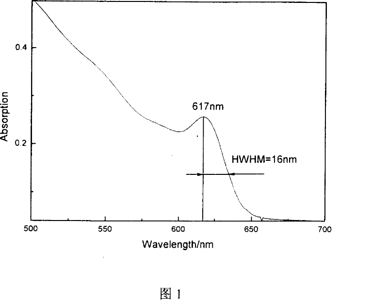
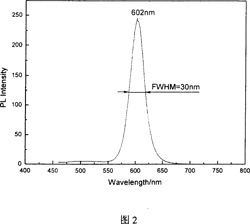
[0039] (3) Continue heating the solution obtained in (1) to 180-270°C. At this temperature, inject the solution obtained in (2) into the above solution, keep the growth temperature at 160-250°C for 5 minutes, and cool down to room temperature. CdSe nanocrystals of about 6 nm were obtained. The ultraviolet-visible spectrum of CdSe nanocrystals obtained under this condition is shown in Fig. 1 . Changing the amount of oleic acid to 6.4mmol and keeping other conditions constant, CdSe nanocrystals with a diameter of about 4.5nm can be obtained. The fluorescence emission spectrum of the CdSe nanocrystals obtained under this condition i...
Embodiment 2
[0041] (1) Take 0.8 mmol of cadmium oxide, 12.6 mmol of oleic acid, and about 0.17 mol of 40 mL of dibutyl maleate, put them in a three-necked flask, pass high-purity Ar gas, stir evenly, and heat to dissolve cadmium oxide to form homogeneous solution.
[0042] (2) Dissolve 0.4 mmol of selenium in 4 mL of about 9 mmol of TOP to prepare a clear solution.
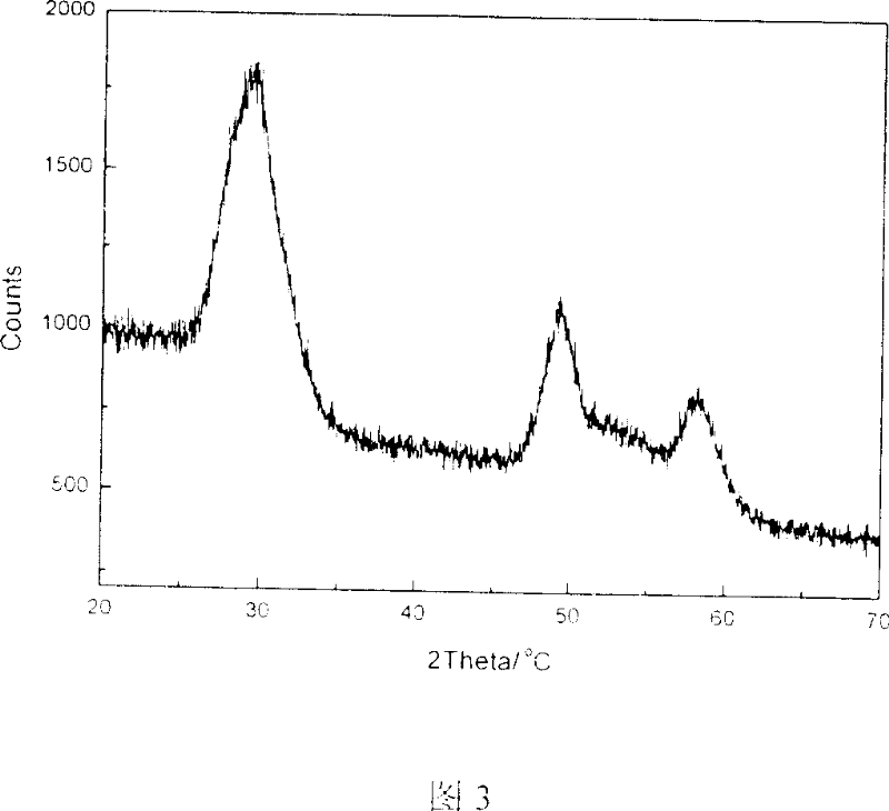
[0043] (3) Continue heating the solution obtained in (1) to 180-270°C. At this temperature, inject the solution obtained in (2) into the above solution, keep the growth temperature at 160-250°C for 60 minutes, and cool down to room temperature. CdSe nanocrystals of about 8 nm were obtained. By changing the amounts of cadmium oxide and selenium to 0.25mmol and 1.25mmol respectively, and keeping other conditions unchanged, CdSe nanocrystals with a diameter of about 5nm can be obtained. The powder diffraction spectrum and transmission electron microscope photos of the CdSe nanocrystals obtained under this condition are shown i...
Embodiment 3
[0045] (1) Take 0.2mmol of cadmium oxide, 3.2mmol of oleic acid, and about 86mmol of 40mL dioctyl p-sebacate, put them in a three-necked flask, pass high-purity N 2 gas, stir evenly, and heat to dissolve cadmium oxide to form a uniform solution
[0046](2) Dissolve 0.4 mmol of selenium in 1.5 mL of about 3.4 mmol of TOP to prepare a clear solution.
[0047] (3) Continue heating the solution obtained in (1) to 180-270°C. At this temperature, inject the solution obtained in (2) into the above solution, keep the growth temperature at 160-250°C for 1-5 minutes, and cool down to room temperature , respectively, 2.5-4nm CdSe nanocrystals can be obtained. The energy dispersive spectrum of the obtained CdSe nanocrystals is shown in FIG. 5 .
PUM
 Abstract
Description
Claims
Application Information