Method for manufacturing silicon chip of ultramicro tension pressure sensor

A technology of pressure sensor and manufacturing method, applied in the field of electronic information

Inactive Publication Date: 2008-12-03
WENZHOU UNIV +2
View PDF4 Cites 0 Cited by
  • Summary
  • Abstract
  • Description
  • Claims
  • Application Information

AI Technical Summary

Problems solved by technology

So far, there have been no foreign reports on piezoresistive pressure sensors with a range below 300Pa, and Honeywell is in the leading position in commercialization, and the lowest range in its product catalog is 1000Pa

Method used


Image

  • Method for manufacturing silicon chip of ultramicro tension pressure sensor
  • Method for manufacturing silicon chip of ultramicro tension pressure sensor
  • Method for manufacturing silicon chip of ultramicro tension pressure sensor

Examples


Embodiment Construction

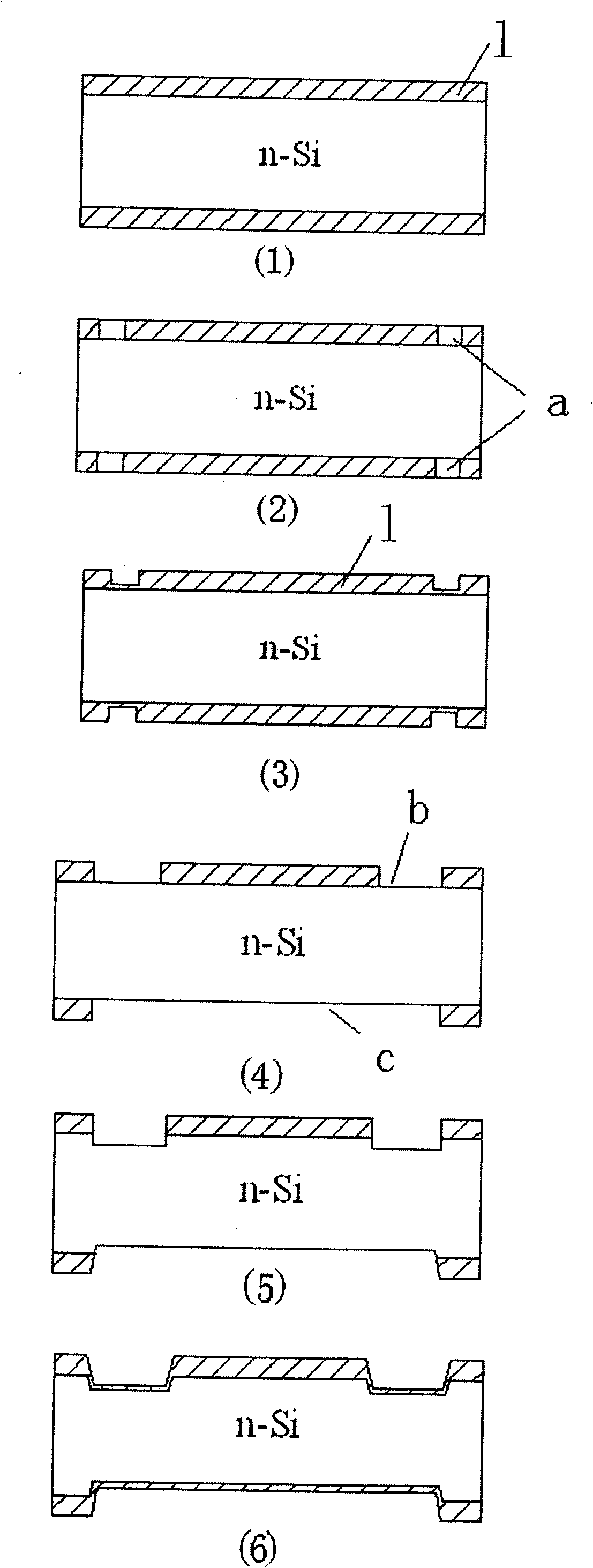
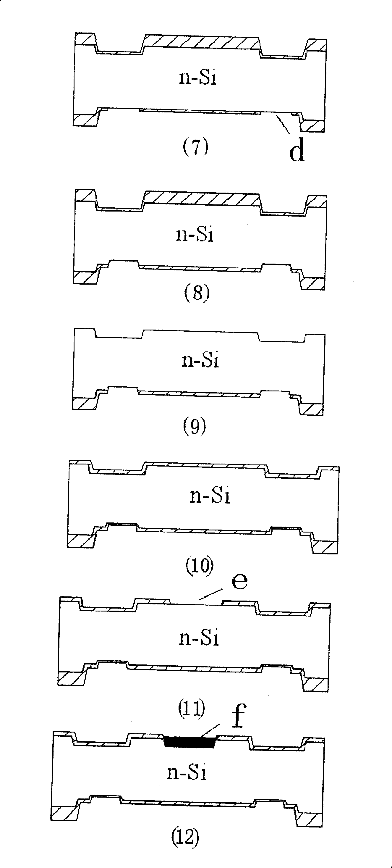
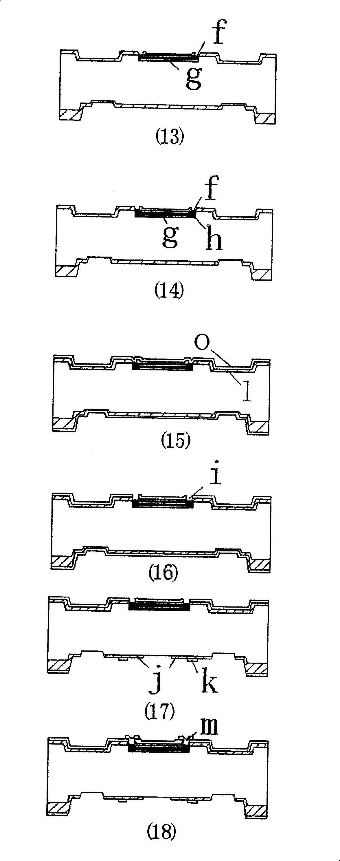
[0035] As the flow chart shown in the accompanying drawing, the original material selected by the present invention is an N-type monocrystalline silicon wafer with double-sided polishing (100) crystal faces, the resistivity is 0.5~5.0Ω cm, and the original thickness of the silicon wafer is 220 ±20μm, the specific production method includes the following steps:

[0036] (1) Oxidation: Put the strictly cleaned silicon wafer into an oxidation furnace, and oxidize both sides of the silicon wafer with oxygen at a temperature of 1150°C. First, dry oxidation for 10 minutes, and then wet oxidation with water vapor for 30 minutes.

[0037] (2) Double-sided lithography alignment marks: double-sided lithography of oxidized silicon wafers to form double-sided alignment marks, wherein the back is coated with glue, the pre-baking temperature is 80°C, and the time is 5 minutes, and the front is coated with glue , the pre-bake temperature is 80°C, and the time is 10 minutes.

[0038] (3) Oxi...


PUM

PropertyMeasurementUnit
electrical resistivityaaaaaaaaaa
Sensitivityaaaaaaaaaa

Abstract

The invention relates to the fabrication method of the ultra-low-pressure sensor silicon chips, which develops the ultra-low-pressure sensor silicon microchips with high sensitivity under the condition of ensuring the high linear accuracy by adopting the combination of the planar process of silicon and process technology of bulk micromachining, adopting the planar process technology of the integrated circuit and anisotropic erosion of silicon, combining the advantages of the beam diaphragm structure and the plane membrane twin islands structure in the pressure sensor chip design and adopting the twin islands-beam-membrane structure to fully concentrate the stress. The method mainly comprises the steps such as oxidation-dual surface lithography alignment mark- oxidation-lithography back large membrane and lithography facade beam zone-back large membrane and facade beam zone erosion- oxidation-lithography back stress unification zone- back stress unification zone erosion-back glue protection and facade rinse SiO2 layer- oxidation- lithography resistance zone-sensing resistor zone boron dope- lithography heavy boron zone-heavy boron-diffusion formed ohm zone-top and back deposit silicon nitride- lithography pin hole- lithography back small island, lithography back large island-facade aluminum coating, etching back aluminum wire and alloyage-entering the corrosion technology process.

Description

technical field [0001] The invention belongs to the field of electronic information, in particular to a method for manufacturing a pressure sensor silicon chip. Background technique [0002] The development of measurement and control technology requires pressure sensors to have smaller ranges and higher resolutions, making pressure sensors more and more important in scientific experiments, industrial automation control, aerodynamics, metrology and other fields. Such as high-resolution testing in scientific experiments, research on the dynamic characteristics of aircraft, missiles, and moving machinery in aerodynamic research, and wind tunnel design for high-rise buildings, etc., secondary air intake systems for new thermal boilers in industrial control, air conditioning, Ultra-clean filtration systems, coal mine gas monitoring systems, etc., and oil and gas and liquefied gas metering in the metering market, all require high-precision pressure sensors with a range of hundreds...

Claims


Application Information

Patent Timeline
Patent Type & Authority Patents(China)
IPC IPC(8): B81C5/00G01L1/18G01L9/06B81C99/00
Inventor 薛伟沈绍群王文襄鲍敏杭王权王冰
Owner WENZHOU UNIV
Why Eureka
Try Eureka