High-layer circuit board and its manufacturing method

A manufacturing method and circuit board technology, which is applied in the direction of multilayer circuit manufacturing, printed circuit parts, structural connection of printed circuits, etc., can solve the problems of low electroplating yield, difficulty in making thick plates, and high friction

Inactive Publication Date: 2009-02-04
陈文祺
View PDF7 Cites 0 Cited by
  • Summary
  • Abstract
  • Description
  • Claims
  • Application Information

AI Technical Summary

Problems solved by technology

[0002] With the development of consumer electronics products with more and more functions and smaller and smaller volumes, the internal printed circuit board (Printed Circuit Board; PCB) is also becoming more and more complex in circuit design and process technology. The density of components on the board is increasing, the layout of thin lines is increasing, and the interconnection density between layers is increasing. In addition, with the application and design trends of mixed-signal integrated circuits becoming more complicated, in addition to considering the problems of the previous circuit technology, With the evolution of its advanced manufacturing process, the difficulties to be solved in the design process have also increased a lot. For high-frequency and high-speed boards with special needs, in order to control their characteristic impedance, a certain thickness of copper foil is required to bear the load, and the thickness of the circuit board also varies with The addition of these forms veritable slabs, which have their own difficulties in making
The traditional printed circuit board uses glass fiber film, and the double-sided board with the circuit has been made, according to the required number of layers, laminated and aligned once to form a multi-layer circuit substrate. However, the traditional process is laminated and aligned. Pressing, drilling and electroplating, etc., when the number of stacked layers of these thick plates is low, they can be manufactured with the current industry technology and process capabilities. However, when the number of layers is higher, the process difficulties will emerge. The tolerance obtained by the alignment increases with the number of lamination layers. In addition, the expansion and contraction ratio of the lamination material (such as glass fiber film) is not easy to control, so that it is easy to dislocate after lamination, causing another error source for lamination; Mechanical drilling may cause too high friction due to too many layers and too thick total thickness, which may cause the drill bit to break the needle easily. In addition, the aspect ratio between the plate thickness and the aperture is too high, which will affect the difficulty of subsequent electroplating or the formation of dog bones and other undesirable phenomena. ; If laser drilling is performed after pressing, the aperture will be too small, and the aspect ratio will be higher than that of mechanical drilling, and the plating yield will be lower; there is also a technology called Build Up Process that has developed rapidly. The concept of traditional multi-layer board sequential lamination (Sequential Laminated) is to add insulating layers and conductor layers to the outside of the core substrate based on double-layer or four-layer boards, and to manufacture conductor lines on the insulating layer, abandoning machine drilling. Type small holes (above 10mil), and use "non-drillable" blind buried micro-vias as the interconnection between build-up layers, and blind holes (Blind Hole) and buried holes (Buried Hole) connected between some layers, It can save the space occupied by through holes on the board surface, so that the limited outer layer area can be used for wiring and welding parts as much as possible. Since the development of multilayer boards with build-up method, more than ten kinds of process technologies have been used in commercial mass production. Such as SLC, FRL, DYCOstrate, Z-Link, ALIVH, HDI, etc., different processes use different materials and substrates, so the hole forming technology is also different, which can be roughly divided into photosensitive hole forming, laser drilling, Various methods such as plasma pitting and chemical pitting
However, the main effect of the layer-build method is to reduce the area occupied by the through-holes and achieve high-density requirements, but it is only suitable for thin plates with a low number of layers and the purpose is light, thin and short. Circuit boards with small pitches and layers of more than 18 layers still have difficulties, such as drilling methods and electrical conduction problems caused by excessively high aspect ratios of drilling holes.

Method used


Image

  • High-layer circuit board and its manufacturing method
  • High-layer circuit board and its manufacturing method
  • High-layer circuit board and its manufacturing method

Examples


Embodiment Construction

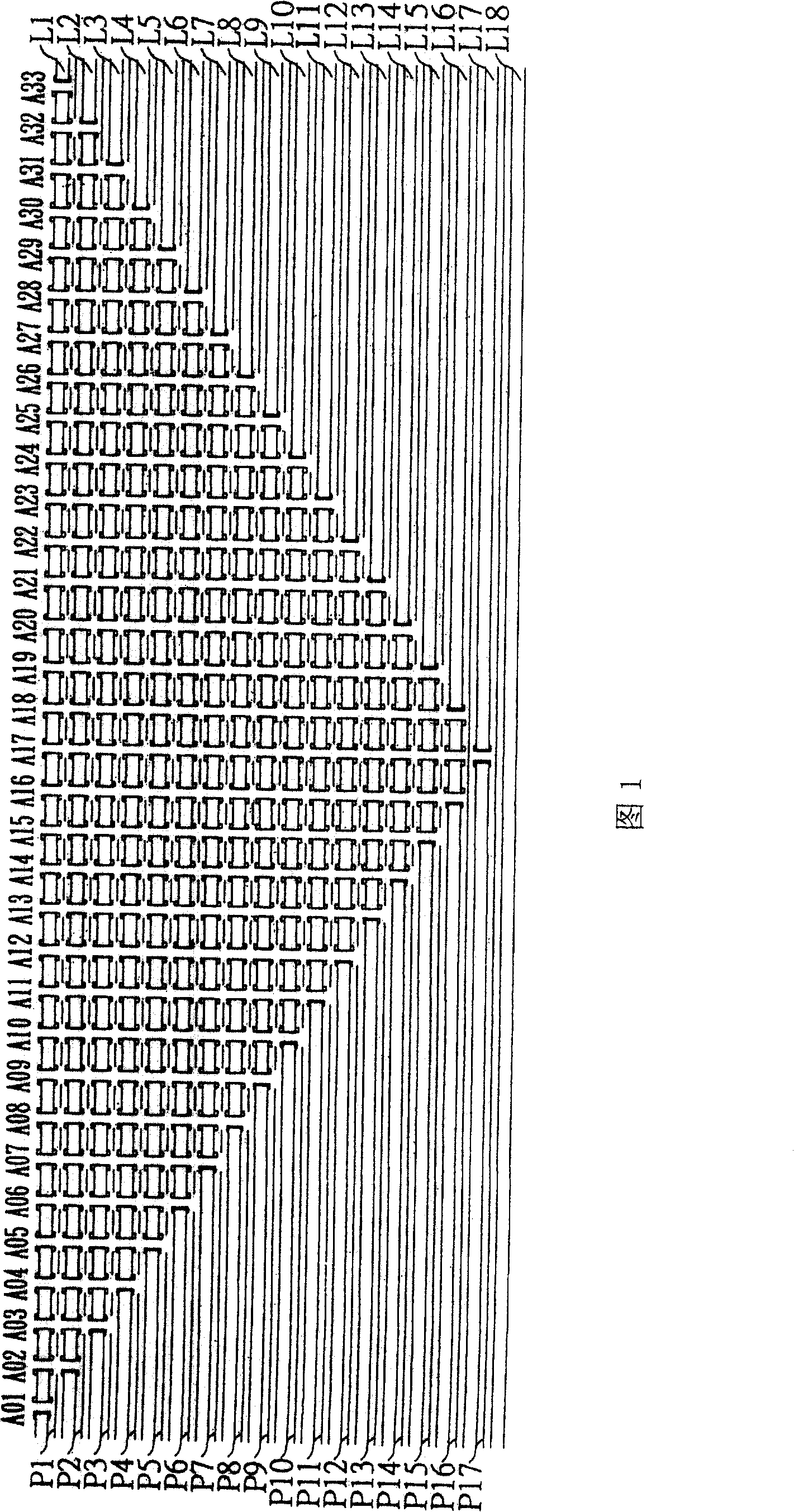
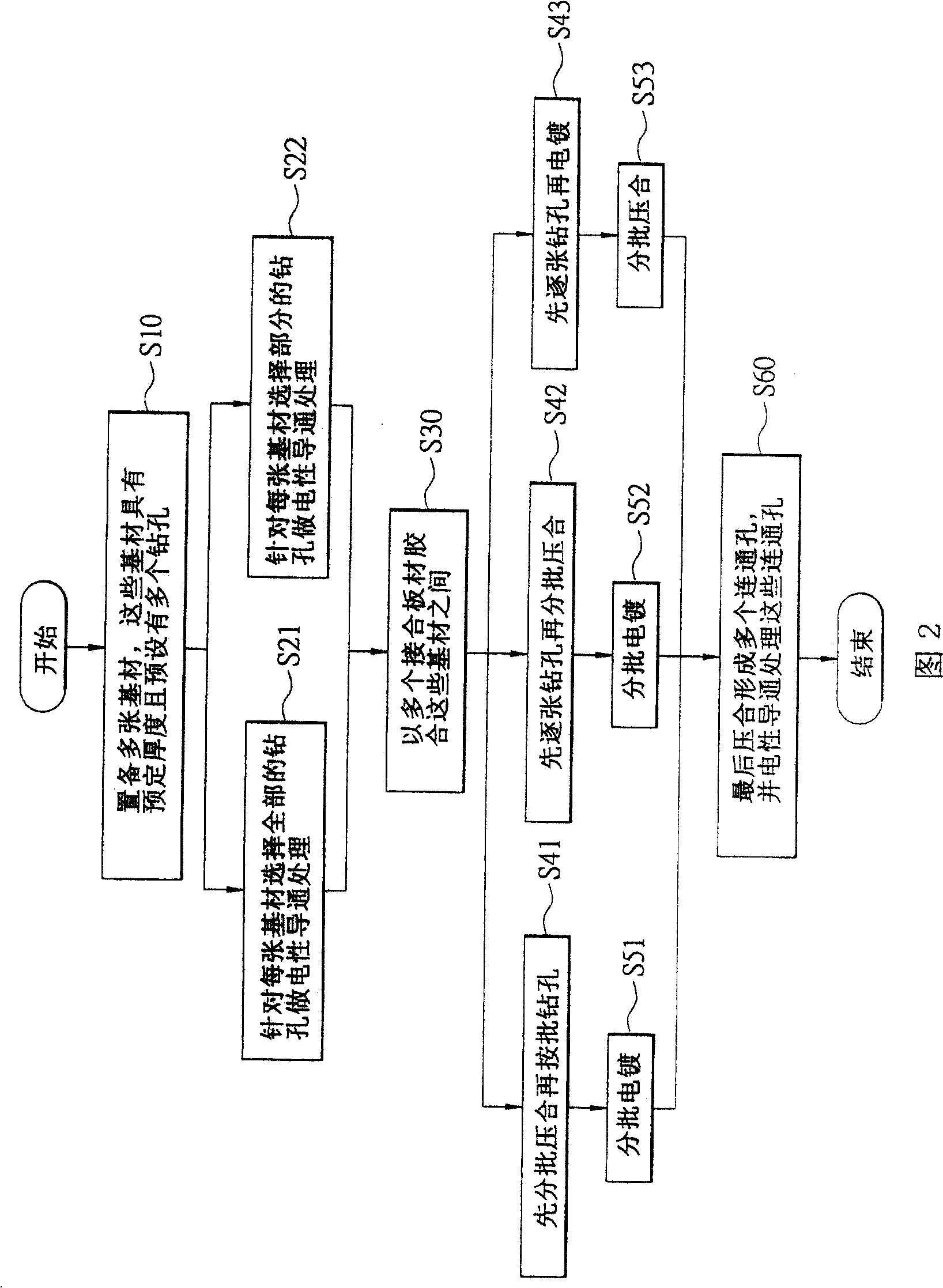
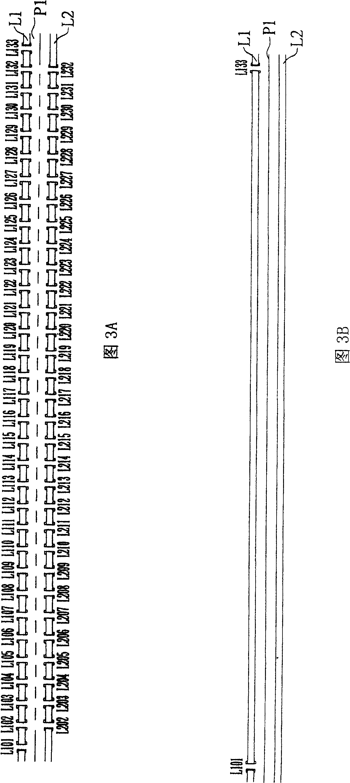
[0019] Please refer to FIG. 1 , the present invention provides a high-layer circuit board with a predetermined thickness of copper foil, a pitch of less than 0.65 mm (may be 0.65-0.01 mm), and more than 18 layers. Pitch refers to the distance between the drilled holes on the circuit board, or the distance between the corresponding chip solder balls. The allowable error range is smaller, and the requirements for process accuracy and process capability are higher. The thickness of copper foil is higher than that of ordinary circuit boards. Once the number of laminated layers is too high, not only is it difficult to align, but it is also difficult to drill holes, and electrical conduction is even more problematic. Therefore, the high-layer circuit board provided by the present invention is a The multi-layer substrate is divided into two or more low-layer multi-layer boards. The number of layers depends on the thickness of the board and the process capability of the machine. It is ...


PUM

PropertyMeasurementUnit
Spacingaaaaaaaaaa

Abstract

The invention relates to a kind of multilayer circuit board and its manufacturing method. It includes multilayer base material and drilled holes distributing on it, which are mutually folding. Every base material includes a copper foil with certain highness. The number of drilled holes increases from lower-layer base material to upper-layer one. The drilled holes become several interconnected holes after base materials fold. The deepness of interconnected holes distributes in V shape from the edge of circuit board to the center of the board. That is to say, the interconnected hole of the board edge is shallowest and the one of board center is deepest. The multi-layer base material can be divided into above two boards, which are combined after manufactured, in order to solve the problem of manufacturing to produce multi-layer circuit board.

Description

technical field [0001] The invention relates to a high-layer circuit board and a manufacturing method thereof, in particular to a high-layer circuit board with a certain thickness and a small pitch of more than 18 layers and a manufacturing method thereof. Background technique [0002] With the development of consumer electronics products with more and more functions and smaller and smaller volumes, the internal printed circuit board (Printed Circuit Board; PCB) is also becoming more and more complex in circuit design and process technology. The density of components on the board is increasing, the layout of thin lines is increasing, and the interconnection density between layers is increasing. In addition, with the application and design trends of mixed-signal integrated circuits becoming more complicated, in addition to considering the problems of the previous circuit technology, With the evolution of its advanced manufacturing process, the difficulties to be solved in the...

Claims


Application Information

Patent Timeline
IPC IPC(8): H05K1/11H05K3/46H05K1/14
Inventor 陈文祺
Owner 陈文祺
Why Eureka
Try Eureka