Making method of self-limited boundary film graphics
A thin-film pattern and boundary technology, which is applied in conductive pattern formation, printed circuit manufacturing, semiconductor/solid-state device manufacturing, etc. good uniformity
- Summary
- Abstract
- Description
- Claims
- Application Information
AI Technical Summary
Problems solved by technology
Method used
Image
Examples
Embodiment 1
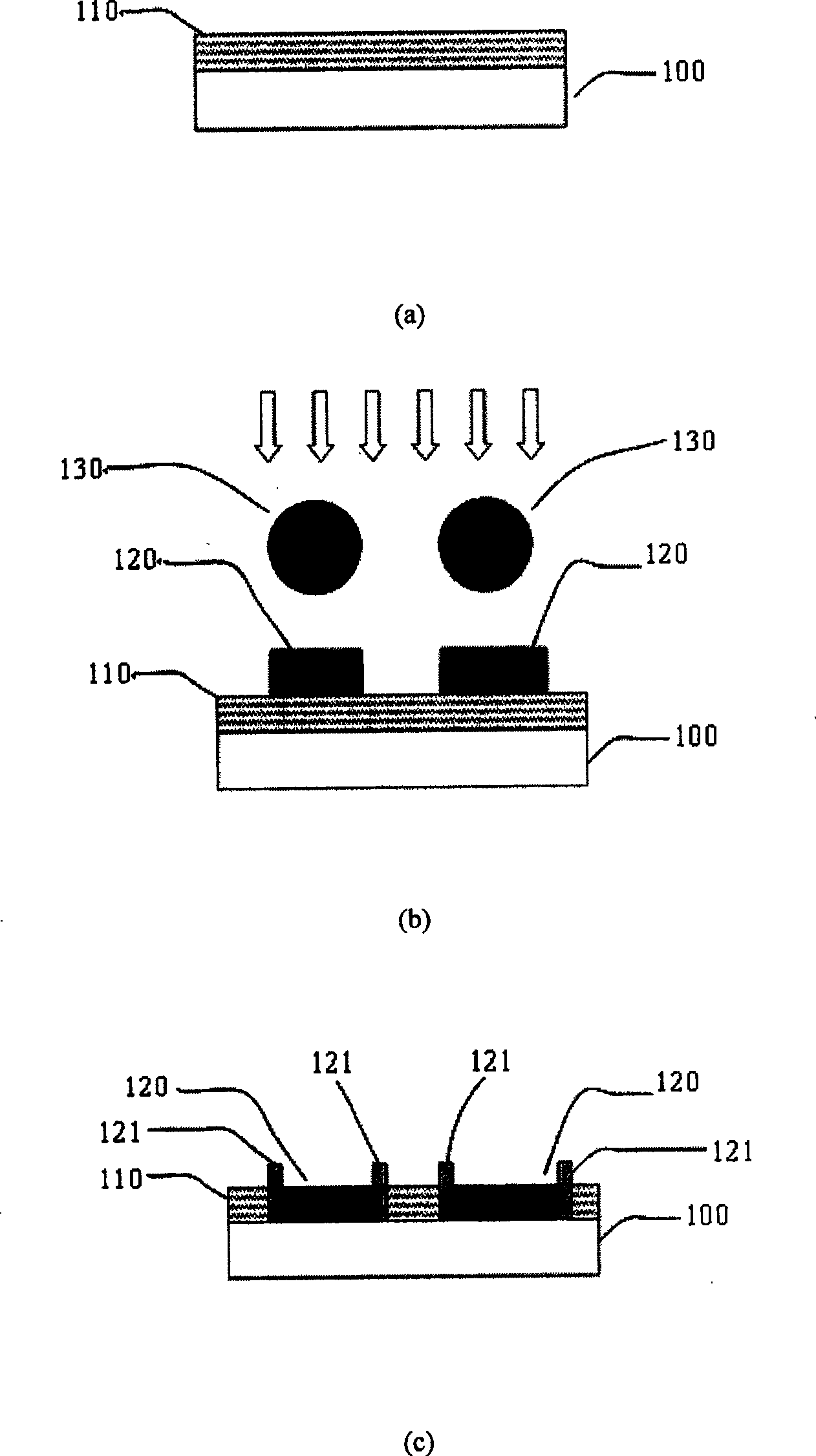
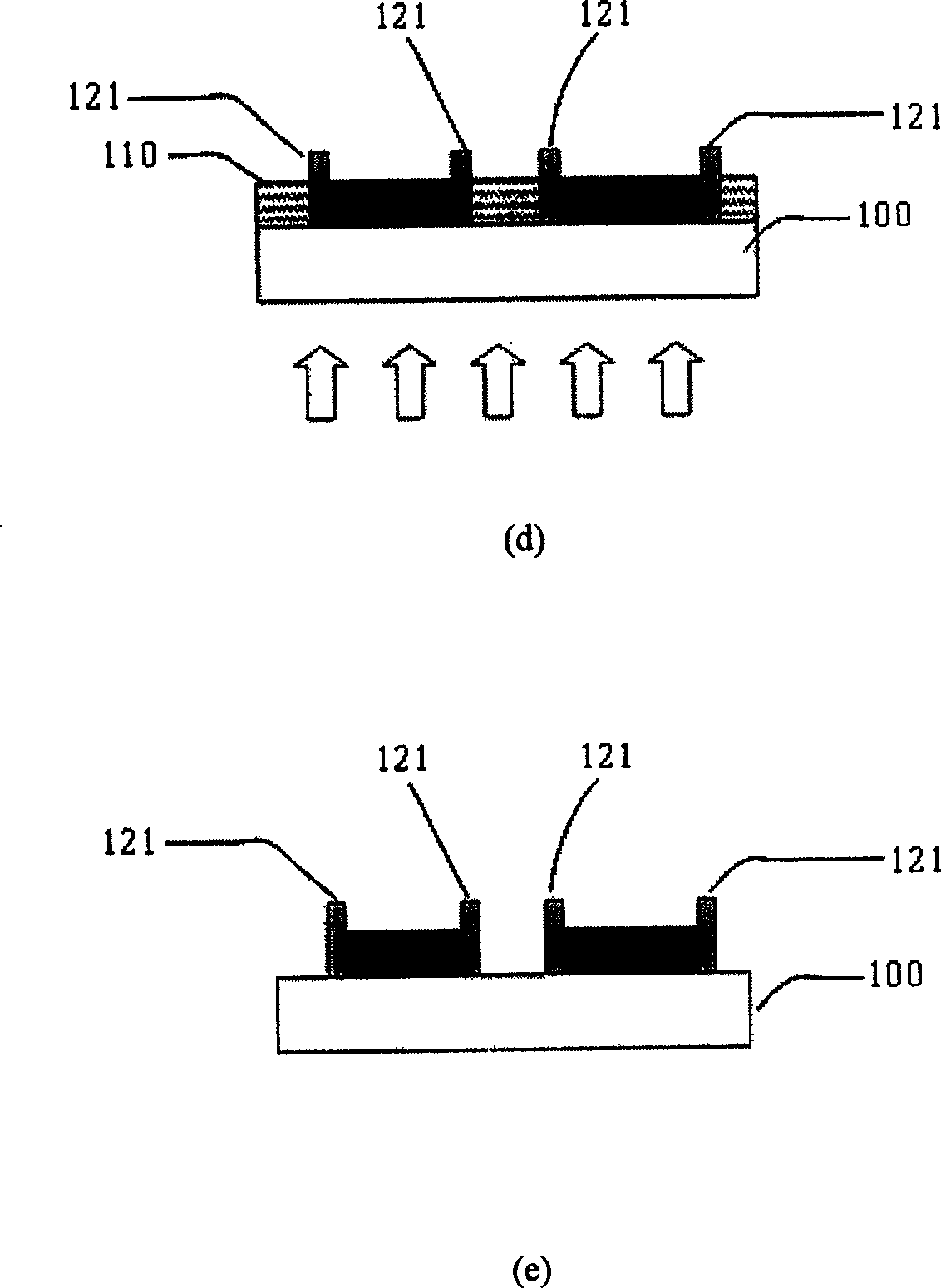
[0029] Example 1: Please refer to figure 2 (a) to figure 2 (e) Flowchart.
[0030] First, please refer to figure 2 As shown in (a), a glass substrate 100 is provided and cleaned with deionized water, and a polymethyl methacrylate (PMMA) barrier layer 110 is preferably formed on the glass substrate 100 . The method for forming the PMMA barrier layer 110 may be spin coating or spinless coating. The silver nanoparticles are then dispersed in an acetone solvent to form a suspension 130 .
[0031] Then, refer to figure 2 As shown in (b), the suspension 130 of silver nanoparticles is deposited on the PMMA barrier layer 110 , and patterned according to the prior design during deposition, here is a circular conductive pattern film 120 . The method of forming the conductive thin film layer 120 may be inkjet printing, or other wet film forming methods. Next, please refer to figure 2 As shown in (c), when the silver nano-suspension 130 is deposited on the top of the PMMA barr...
Embodiment 2
[0032] Example 2, please also refer to figure 2 (a) to figure 2 (e) Flowchart.
[0033] First please refer to figure 2 As shown in (a), a glass substrate 100 is provided and cleaned with deionized water. A polyimide (PI) barrier layer 110 is formed on the glass substrate 100 , and the method for forming the barrier layer 110 may be spin coating (Spin Coating) or non-spin coating (Spinless Coating). The silver nanoparticles are then dispersed in a chloroform solvent to form a suspension 130 . Then, refer to figure 2 As shown in (b), the suspension 130 of silver nanoparticles is deposited on the polyimide barrier layer 110, and is patterned according to the prior design during deposition, which is a rectangle here. The method of forming the rectangular conductive thin film layer 120 may be inkjet printing, or other wet film forming methods.
[0034] Then please refer to figure 2 (c), when the silver nanosuspension 130 is deposited on the polyimide barrier layer of th...
PUM
| Property | Measurement | Unit |
|---|---|---|
| thickness | aaaaa | aaaaa |
| thickness | aaaaa | aaaaa |
Abstract
Description
Claims
Application Information


