Nanometer oxide porous membrane electrode and preparing method and application thereof
A nano-oxide and porous film technology, applied in capacitor electrodes, circuits, photovoltaic power generation, etc., can solve the problems of energy consumption, time-consuming, unusable, etc., and achieve the effect of uniform film layer, simple preparation process and energy saving.
- Summary
- Abstract
- Description
- Claims
- Application Information
AI Technical Summary
Problems solved by technology
Method used
Image
Examples
Embodiment 1
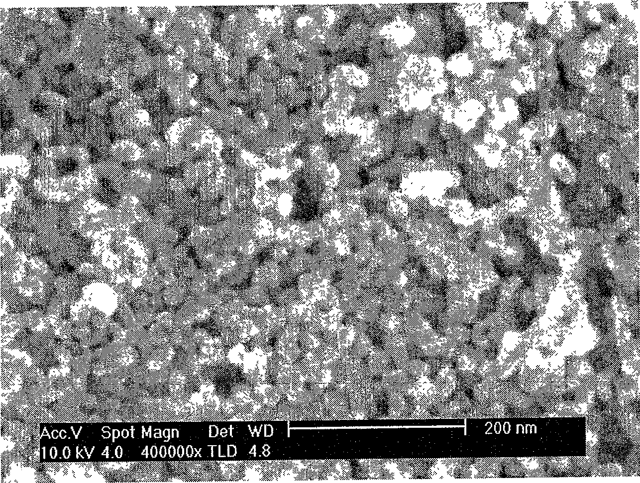
[0036] Present embodiment is made on the FTO glass substrate and is coated with 2 layers of nano-semiconductor material ZnO layers, obtains nano-semiconductor material ZnO porous film, and the aperture of irregular hole is 0.01-2 nanometer; Film thickness is at 1 micron, and film porosity is at 30% , the specific surface area can be 40 square meters per gram.
[0037] The concrete method that present embodiment makes nano-semiconductor material ZnO porous film is as follows:
[0038] 1) preparation solution concentration is the aqueous acetic acid solution of 0.2wt%;
[0039] 2) Mix 3g of ZnO nanopowder (with a particle size of 20 nanometers) with 15g of acetic acid aqueous solution, grind and mix it on a ball mill for 1 hour, then leave it at room temperature for 30 minutes to obtain a nanometer ZnO slurry;
[0040] 3) on the FTO glass substrate, apply the nano-ZnO slurry film prepared in step 2) by scraping, and apply it for 3 times to obtain a film layer with the same semi...
Embodiment 2
[0043] Present embodiment is made on the FTO glass substrate and is coated with 3 layers of nano-semiconductor material ZnO layers, obtains nano-semiconductor material ZnO porous film, and the aperture of irregular hole is 1 nanometer; Film thickness is at 4 microns, and film porosity is at 40%, ratio The surface area can be in the range of 60 m2 / g.
[0044] The concrete method that present embodiment makes nano-semiconductor material ZnO porous film is as follows:
[0045] 1) preparation solution concentration is the acetic acid aqueous solution of 1wt%;
[0046] 2) Mix 3g of ZnO nanopowder (with a particle size of 20 nanometers) with 8g of acetic acid aqueous solution, grind and mix it on a ball mill for 1 hour, then leave it at room temperature for 30 minutes to obtain a nanometer ZnO slurry;
[0047] 3) on the FTO glass substrate, apply the nano-ZnO slurry film prepared in step 2) by scraping, and apply it for 3 times to obtain a film layer with the same semiconductor. Af...
Embodiment 3
[0050] Present embodiment is made on the FTO glass substrate and is coated with 3 layers of nano-semiconductor material ZnO layers, obtains nano-semiconductor material ZnO porous film, and the aperture of irregular hole is 0.1-5 nanometer; Film thickness is at 12 microns, and film porosity is at 40% , the specific surface area can be 60 square meters per gram.
[0051] The concrete method that present embodiment makes nano-semiconductor material ZnO porous film is as follows:
[0052] 1) preparation solution concentration is the acetic acid aqueous solution of 3wt%;
[0053] 2) Mix 3g of ZnO nanopowder (with a particle size of 20 nanometers) with 3g of acetic acid aqueous solution, grind and mix on a ball mill for 1 hour, then leave at room temperature for 30 minutes to obtain a nanometer ZnO slurry;
[0054] 3) On the FTO glass substrate, apply the nano-ZnO slurry film prepared in step 2) by scraping, and apply it for 3 times to obtain a film layer with the same semiconducto...
PUM
| Property | Measurement | Unit |
|---|---|---|
| particle diameter | aaaaa | aaaaa |
| thickness | aaaaa | aaaaa |
| specific surface area | aaaaa | aaaaa |
Abstract
Description
Claims
Application Information
 - R&D
- Intellectual Property
- Life Sciences
- Materials
- Tech Scout
- Unparalleled Data Quality
- Higher Quality Content
- 60% Fewer Hallucinations
Browse by: Latest US Patents, China's latest patents, Technical Efficacy Thesaurus, Application Domain, Technology Topic, Popular Technical Reports.
© 2025 PatSnap. All rights reserved.Legal|Privacy policy|Modern Slavery Act Transparency Statement|Sitemap|About US| Contact US: help@patsnap.com


