Method for making embedded resistor in semiconductor wafer
A technology of embedded resistors and manufacturing methods, which is applied in semiconductor/solid-state device manufacturing, semiconductor devices, electric solid-state devices, etc., can solve the problems of IO speed delay, damage to semiconductor chip performance, etc., to prevent delay and reduce occupied space , Improve the effect of packaging density
- Summary
- Abstract
- Description
- Claims
- Application Information
AI Technical Summary
Problems solved by technology
Method used
Image


Examples
Embodiment 1
[0076] In this embodiment, the embedded resistors are fabricated in the semiconductor wafer during the process of forming solder bumps on the semiconductor wafer. Its production process is as follows:
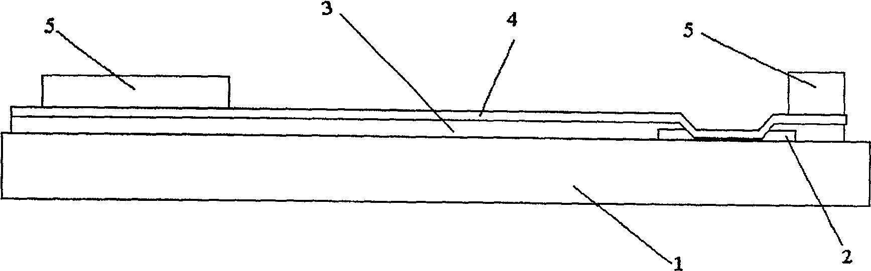
[0077] Carry out sequentially on the semiconductor wafer 1 that has been formed with the semiconductor device device structure and the aluminum pad 2:
[0078] 1) if figure 1 As shown, a benzocyclobutene material is coated as a passivation layer 3, followed by exposure, development, and curing in sequence;
[0079] 2) if figure 2 Shown, with physical vapor deposition method, sputter deposition multilayer metal film layer chromium / copper (Cr / Cu) layer 4, wherein, first deposit chromium layer 41, deposit copper layer 42 then;
[0080] 3) if image 3 As shown, the first photoresist layer 5 is coated, exposed, developed, and firm film layer is formed to form a photoresist pattern for the next process step;
[0081] 4) if Figure 4 As shown, the metal film layer 6 (copper lay...
Embodiment 2
[0091] In this embodiment, in the process of forming gold bumps on the semiconductor wafer, the embedded resistor is manufactured in the semiconductor wafer, and the manufacturing process is as follows:
[0092] Carry out sequentially on the semiconductor wafer 1 that has been formed with the semiconductor device structure and the aluminum pad 2:
[0093] 1) can refer to embodiment 1 figure 1 As shown, coating benzocyclobutene or polyimide material as passivation layer 3, and then sequentially carry out exposure, development, curing;
[0094] 2) can refer to embodiment 1 figure 2 As shown, it is only different from the deposited material of embodiment 1. This embodiment uses the physical vapor deposition method to sputter deposit a multilayer metal film layer titanium tungsten / gold (TiW / Au) layer 4', wherein, Deposit titanium and tungsten first, then deposit gold;
[0095] 3) with reference to Example 1 image 3 As shown, the first photoresist layer 5 is coated, exposed, ...
PUM
 Abstract
Description
Claims
Application Information
 - R&D
- Intellectual Property
- Life Sciences
- Materials
- Tech Scout
- Unparalleled Data Quality
- Higher Quality Content
- 60% Fewer Hallucinations
Browse by: Latest US Patents, China's latest patents, Technical Efficacy Thesaurus, Application Domain, Technology Topic, Popular Technical Reports.
© 2025 PatSnap. All rights reserved.Legal|Privacy policy|Modern Slavery Act Transparency Statement|Sitemap|About US| Contact US: help@patsnap.com