A PIN room temperature nucleus radiation detector and its making method

A nuclear radiation detector and room temperature technology, applied in semiconductor devices, electrical components, circuits, etc., can solve the problems of low thermal conductivity of CZT crystal materials, complicated preparation process, and increase the cost of detector manufacturing, and achieve good mechanical properties and chemical properties. Stability, mature material growth process, and the effect of eliminating the overlay photolithography process

Inactive Publication Date: 2009-12-09
SUZHOU INST OF NANO TECH & NANO BIONICS CHINESE ACEDEMY OF SCI
View PDF4 Cites 0 Cited by
  • Summary
  • Abstract
  • Description
  • Claims
  • Application Information

AI Technical Summary

Problems solved by technology

[0004] At present, the CdZnTe (CZT) room temperature nuclear radiation detector is the most researched. The United States, Russia and other countries have commercialized the CZT crystal material and its detector. However, the crystal material has the following problems: ① Due to the thermal conductivity of the CZT crystal material It is extremely low, and its stacking defect formation energy is small, so that during the crystal growth process, factors such as temperature fluctuations can easily cause the appearance of twins; ②Due to its low critical shear stress, it is easy to generate dislocations; ③Its constituent elements Among them, the vapor partial pressure of Cd is much higher than that of the other two components, and it is easy to cause the melt to be rich in Te; ④ During the cooling process of its crystal growth, the width of the solid solution zone existing at high temperature is at room temperature will shrink to "0", it is easy to form Te precipitation / inclusion, which will affect the material performance; therefore, it is difficult to prepare high-quality CZT crystal and its detector, and its cost is also very expensive
However, the thickness of existing GaN ultraviolet detectors is only 1-2 microns, which is not suitable for room temperature nuclear radiation detection
[0007] On the other hand, in the prior art, the unidirectional growth process is used in the preparation of the detector, and the contact electrode is prepared by multi-step photolithography, so the preparation process is relatively complicated, which also increases the production cost of the detector.

Method used


Image

  • A PIN room temperature nucleus radiation detector and its making method

Examples


Embodiment 1

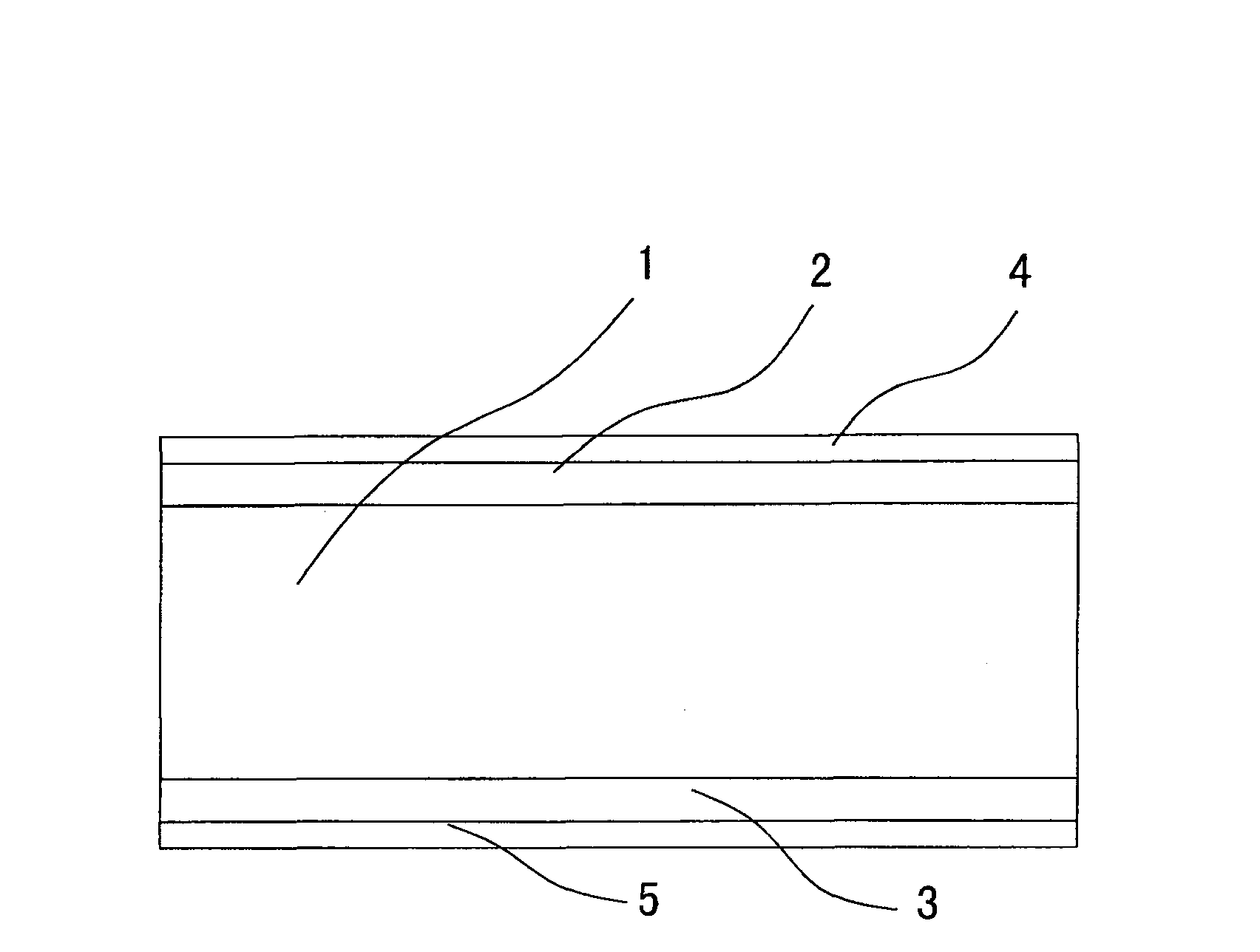
[0033] Embodiment one: see attached figure 1 As shown, a PIN-type GaN room temperature nuclear radiation detector includes a GaN substrate 1, an n-type doped layer 2, a p-type doped layer 3 and two contact electrodes 4, 5, and the n-type doped layer 2 It is fabricated on one side of the GaN substrate 1, the p-type doped layer 3 is fabricated on the other side of the GaN substrate 1, and the contact electrodes 4 and 5 are respectively fabricated on the outer surfaces of the n-type and p-type doped layers. The GaN substrate 1 is a GaN single crystal thick film with a thickness of 100-200um and a resistivity of 10 6 ~10 9 Ω cm, dislocation density less than 10 6 cm -2 ; The thickness of the n-type doped layer 2 is 2um, and the thickness of the p-type doped layer 3 is 2um.

[0034] The preparation method of the PIN type GaN room temperature nuclear radiation detector of this embodiment comprises the following steps:

[0035] 1) A GaN film with a thickness of 3um is grown on a s...

Embodiment 2

[0040] Embodiment 2: A method for preparing a PIN type GaN room temperature nuclear radiation detector, comprising the following steps:

[0041] 1) A GaN film with a thickness of 3um is grown on a sapphire substrate by MOCVD epitaxy to obtain a smooth surface GaN film with high crystal quality;

[0042] 2) Using the above-mentioned GaN thin film as a new substrate, use the HVPE epitaxy method to grow a thick GaN single crystal film with a thickness of 100-200um;

[0043] 3) Si ions were implanted on one side of the above-mentioned GaN single crystal thick film substrate, and the implanted ion concentration was 5×10 18 / cm 3 ~5×10 19 / cm 3 , to form an n-type doped layer with a thickness of 1um; turn over the above substrate, and implant Mg ions on the other side of the substrate, and the implanted ion concentration is 5×10 18 / cm 3 ~5×10 19 / cm 3 , forming a P-type doped layer with a thickness of 1um;

[0044] 4) Deposit 10nm / 20nm Ti / Au on the above-mentioned n-type do...


PUM


Abstract

The invention discloses a PIN type room temperature nuclear radiation detector, comprising a GaN substrate, an n-type doped layer, a p-type doped layer and two contact electrodes, characterized in that the GaN substrate is a thick film structure, Its thickness is 100um~200um, the n-type doped layer is a GaN film doped with silicon, which is made on one side of the GaN substrate, and the p-type doped layer is a GaN film doped with magnesium, made on a GaN substrate. On the other side of the substrate, two contact electrodes are respectively fabricated on the outer surfaces of the n-type doped layer and the p-type doped layer. The room temperature nuclear radiation detector of the present invention has good room temperature sensitivity, detection efficiency and stability, and is more suitable for the detection field of strong radiation fields; meanwhile, the manufacturing process of the present invention is simple and low in cost, and is suitable for industrialization.

Description

technical field [0001] The invention relates to a nuclear radiation detector and a preparation method thereof, in particular to a PIN room temperature nuclear radiation detector and a preparation method thereof. Background technique [0002] Room temperature nuclear radiation detectors are a new type of detectors developed after gas detectors and scintillator detectors. They have high room temperature sensitivity, low noise, wide response spectrum, short pulse time, high detection efficiency, and radiation damage resistance. Strong, high stability and other advantages, it has a wide range of applications in the fields of environmental monitoring, nuclear medicine, industrial non-destructive testing, safety inspection, nuclear weapon penetration, aerospace, astrophysics and high-energy physics, and has become a frontier research hotspot in the modern high-tech field one. [0003] However, since room temperature nuclear radiation detectors are required to work at room tempera...

Claims


Application Information

Patent Timeline
Patent Type & Authority Patents(China)
IPC IPC(8): H01L31/117H01L31/18
Inventor 陆敏
Owner SUZHOU INST OF NANO TECH & NANO BIONICS CHINESE ACEDEMY OF SCI
Why Eureka
Try Eureka