Close-shaped magnetic multi-layer film and preparation method and use thereof
A multi-layer film and magnetic technology, applied in the direction of spin-exchange coupled multi-layer film, magnetic film to substrate, magnetic layer, etc., can solve the problem of complex structure design and preparation of memory cells, increasing free layer inversion issues such as field and power consumption
- Summary
- Abstract
- Description
- Claims
- Application Information
AI Technical Summary
Problems solved by technology
Method used
Image

Examples
Embodiment 1
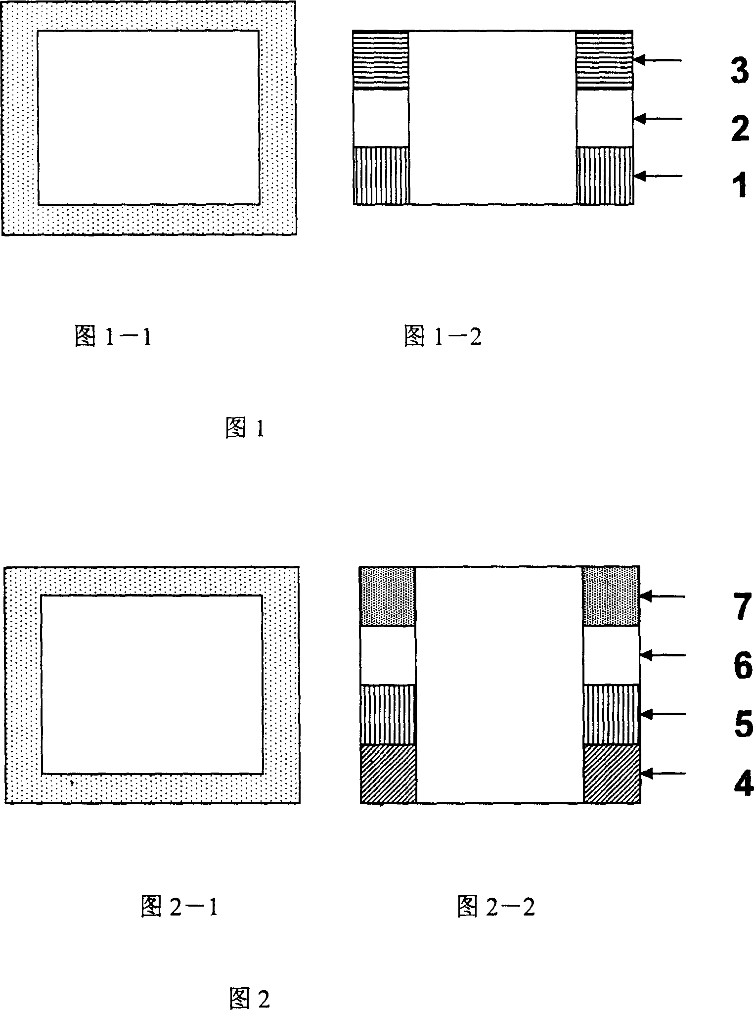
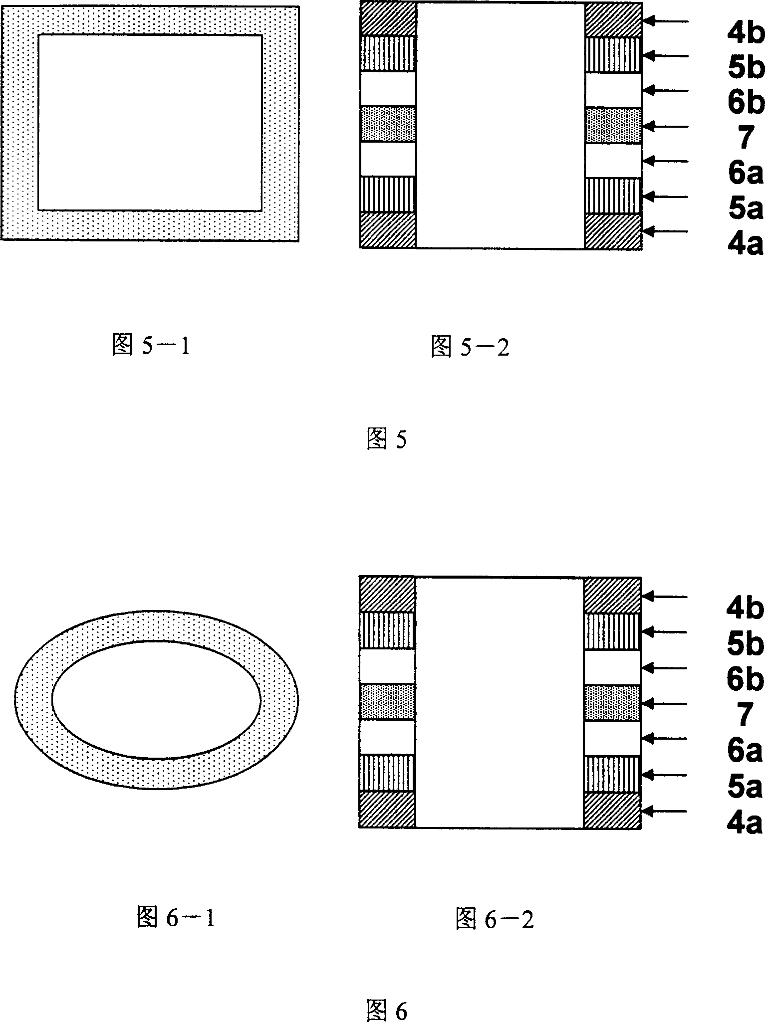
[0050] Example 1. Preparation of non-pinning closed rectangular annular magnetic multilayer film
[0051] Using high-vacuum magnetron sputtering equipment in the 1mm thick SiO cleaned by conventional methods 2 On the Si substrate, the lower buffer conductive layer Au with a thickness of 2nm, the hard magnetic layer (HFM) Co with a thickness of 3nm, the intermediate layer (I1) Cu with a thickness of 1nm, and the soft magnetic layer (SFM) with a thickness of 1nm were deposited sequentially. Co and a cap layer Ru with a thickness of 4 nm. The growth conditions of the above-mentioned magnetic multilayer film: prepared vacuum: 5×10 -7 Pa; pressure of high-purity argon gas for sputtering: 0.07 Pa; sputtering power: 120 watts; sample holder rotation rate: 20rmp; growth temperature: room temperature; Rate; when depositing hard and soft magnetic layers, a 500e plane induced magnetic field is applied. The deposited magnetic multilayer film adopts the micro-processing technology in th...
Embodiment 2
[0052] Example 2, Preparation of non-pinning closed rectangular ring-shaped magnetic multilayer film
[0053] Using high-vacuum magnetron sputtering equipment in the 1mm thick SiO cleaned by conventional methods 2 On the Si substrate, the lower buffer conductive layer Au with a thickness of 2nm, the hard magnetic layer (HFM) Co with a thickness of 3nm, the intermediate layer (I1) Cu with a thickness of 1nm, and the soft magnetic layer (SFM) with a thickness of 1nm were deposited sequentially. Co and a cap layer Ru with a thickness of 4 nm. The growth conditions of the above-mentioned magnetic multilayer film: prepared vacuum: 5×10 -7 Pa; high-purity argon gas pressure for sputtering: 0.07 Pa; sputtering power: 120 watts; sample holder rotation rate: 20rmp; growth temperature: room temperature; Rate; when depositing hard magnetic layer and soft magnetic layer, apply a 50Oe plane induced magnetic field. The deposited magnetic multilayer film adopts the micro-processing techno...
Embodiment 3
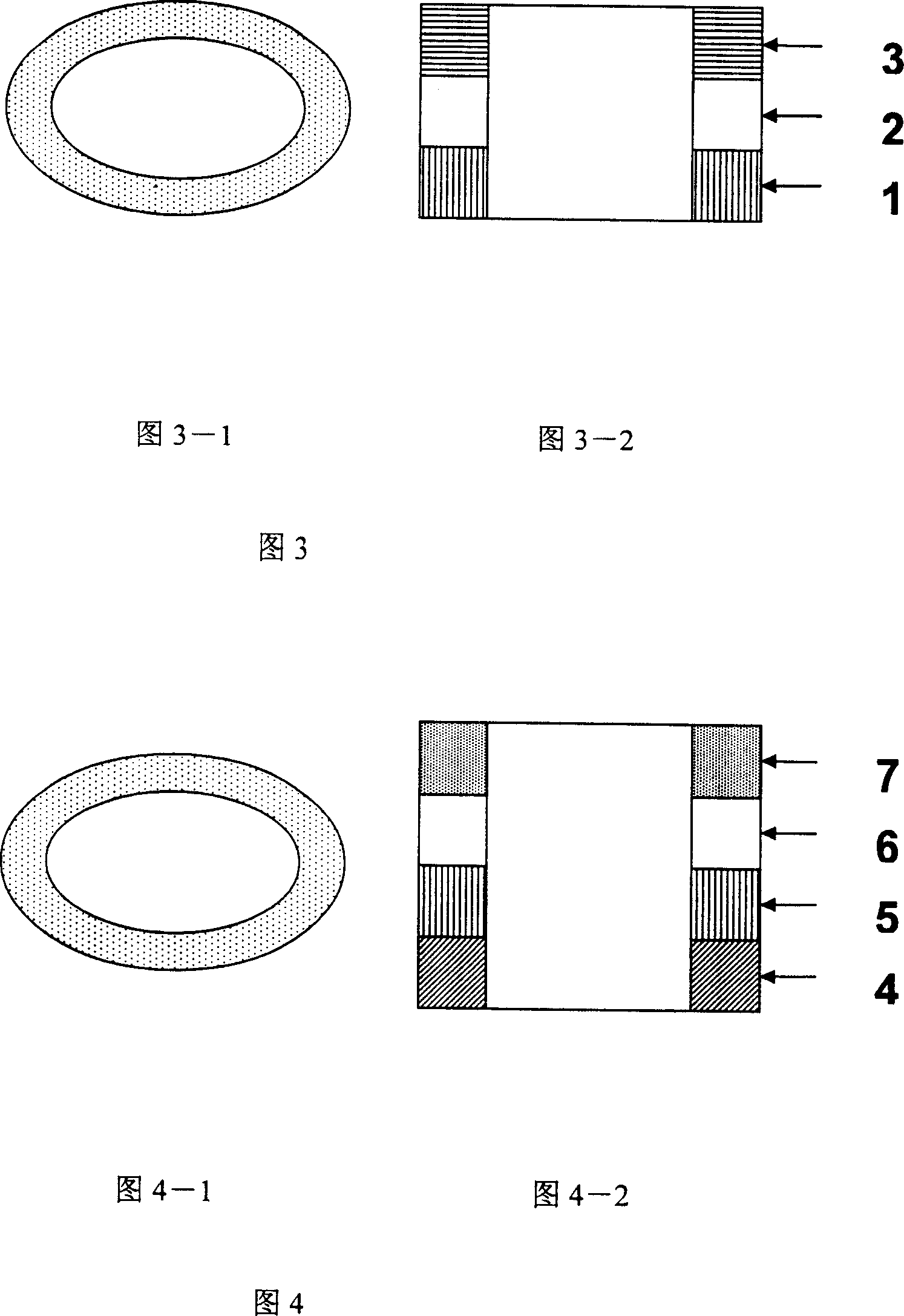
[0054] Example 3, Preparation of a pinned closed rectangular ring-shaped magnetic multilayer film
[0055] Using high vacuum magnetron sputtering equipment to clean 0.8mm thick Si / SiO by conventional methods 2 The lower buffer conductive layer Au with a thickness of 2 nm, the antiferromagnetic pinning layer (AFM) IrMn with a thickness of 10 nm, and the pinned magnetic layer (FM1) Co with a thickness of 3 nm were sequentially deposited on the substrate. 90 Fe 10 ; then deposit 1nm of Al, the insulating layer formed through plasma oxidation for 50 seconds as the intermediate layer (I2); on this intermediate layer, the free soft magnetic layer (FM2) Co with a thickness of 3nm is deposited successively 90 Fe 10 and a capping layer of Au with a thickness of 2 nm. The growth conditions of the above-mentioned magnetic multilayer film: prepared vacuum: 5×10 -7 Pa; high-purity argon gas pressure for sputtering: 0.07 Pa; sputtering power: 120 watts; sample holder rotation rate: 20rm...
PUM
| Property | Measurement | Unit |
|---|---|---|
| width | aaaaa | aaaaa |
| width | aaaaa | aaaaa |
| thickness | aaaaa | aaaaa |
Abstract
Description
Claims
Application Information
 - R&D
- Intellectual Property
- Life Sciences
- Materials
- Tech Scout
- Unparalleled Data Quality
- Higher Quality Content
- 60% Fewer Hallucinations
Browse by: Latest US Patents, China's latest patents, Technical Efficacy Thesaurus, Application Domain, Technology Topic, Popular Technical Reports.
© 2025 PatSnap. All rights reserved.Legal|Privacy policy|Modern Slavery Act Transparency Statement|Sitemap|About US| Contact US: help@patsnap.com