Integrated photon crystal double waveguide back coupling fluid refractive index sensor

A technology of refractive index sensor and photonic crystal, which is applied in the field of integrated optoelectronics, can solve the problems of high noise, cannot be integrated in plane, and is difficult to use, and achieves the effect of high sensitivity characteristics.

Inactive Publication Date: 2007-08-22
TSINGHUA UNIV
View PDF0 Cites 34 Cited by
  • Summary
  • Abstract
  • Description
  • Claims
  • Application Information

AI Technical Summary

Problems solved by technology

[0004] At present, the microcavity structure is mostly used for the detection and sensing of the refractive index of a small amount of fluid using the photonic crystal structure. This structure requires an external pump light. The detected optical signal is scattered upward perpendicular to the surface, which has large noise, It is difficult to be practical due to the shortcomings of not being able to planar integration

Method used


Image

  • Integrated photon crystal double waveguide back coupling fluid refractive index sensor
  • Integrated photon crystal double waveguide back coupling fluid refractive index sensor
  • Integrated photon crystal double waveguide back coupling fluid refractive index sensor

Examples


Embodiment 1

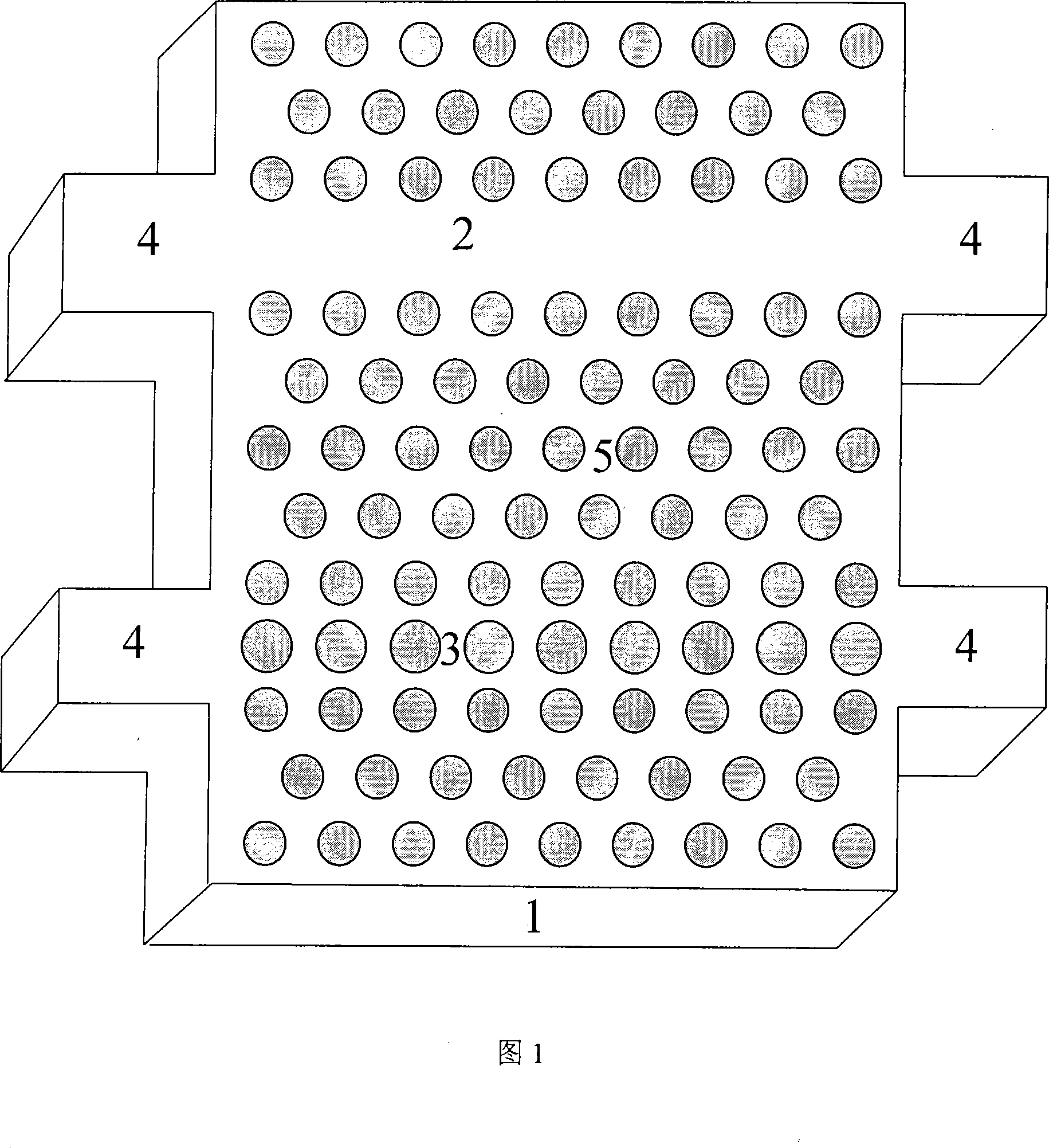
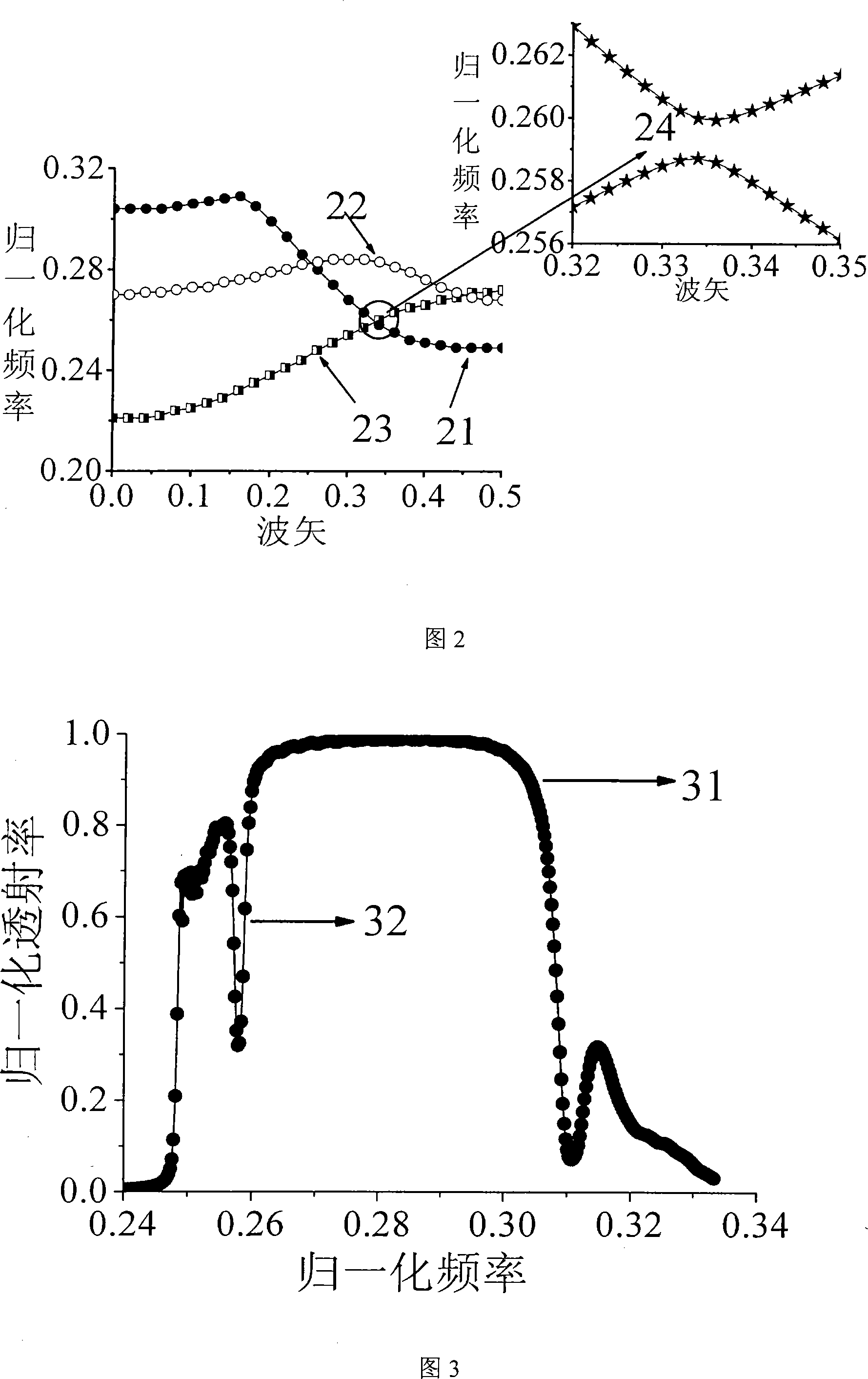
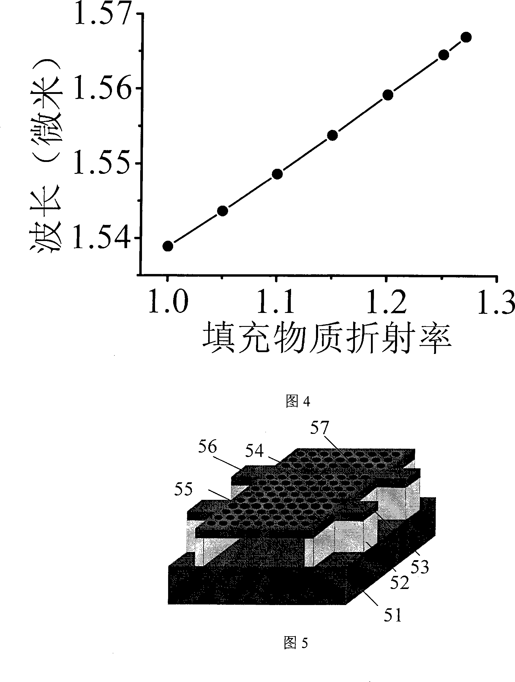
[0030] The structure of the fluid refractive index sensor based on photonic crystal dual-waveguide reverse coupling that can be integrated with the light source of the present invention is shown in FIG. 5 . Select Si-SiO 2 -SOI substrate wafer made of Si, in which SiO 2 The layer thickness is 2 μm, and the upper Si thickness is 220 nm. The connecting waveguide 56 and the 2-dimensional photonic crystal periodic hole structure 57 are fabricated on the uppermost Si plate 53 by electron beam exposure and dry etching, and a double waveguide structure 54, 55 is formed. Removal of a portion of SiO by selective wet etching 2 layer, leaving the SiO 2 The layer is the bridge support structure 52 . When the light field introduced by the connecting waveguide 56 passes through the through-waveguide 54, due to the reverse coupling effect with the coupling waveguide 55, the transmission spectrum shown in Figure 3 will be observed at the output connecting waveguide, and the transmission s...

Embodiment 2

[0032]The structure of the fluid refractive index sensor based on photonic crystal dual-waveguide reverse coupling that can be integrated with the light source of the present invention is shown in FIG. 6 . A substrate 61 of GaAs material is selected, and a 2 μm AlGaInP sacrificial layer and a 220 nm GaAs waveguide layer are grown thereon. Electron beam exposure and dry etching are used to fabricate a connecting waveguide 66 and a 2-dimensional photonic crystal periodic hole structure 67 on the uppermost GaAs slab 63 to form dual waveguide structures 64 and 65 . Part of the AlGaInP layer is removed by selective wet etching, and the remaining AlGaInP layer is the bridge support structure 62 . When the light field introduced by the connecting waveguide 66 passes through the straight-through waveguide 64, due to the reverse coupling effect with the coupling waveguide 65, the transmission spectrum shown in Figure 3 will be observed at the output connecting waveguide, and the transm...

Embodiment 3

[0034] The structure of the fluid refractive index sensor based on photonic crystal dual-waveguide reverse coupling that can be integrated with the light source of the present invention is shown in FIG. 7 . A substrate 71 of InP material is selected, and a 2 μm InGaAsP sacrificial layer and a 220 nm InP waveguide layer are grown thereon. The connecting waveguide 76 and the 2-dimensional photonic crystal periodic hole structure 77 are fabricated on the uppermost InP plate 73 by electron beam exposure and dry etching, and a double waveguide structure 74, 75 is formed. A part of the InGaAsP layer is removed by selective wet etching, and the remaining InGaAsP layer is the bridge support structure 72 . When the light field introduced by the connecting waveguide 76 passes through the through-waveguide 74, due to the reverse coupling effect with the coupling waveguide 75, the transmission spectrum shown in Figure 3 will be observed at the output connecting waveguide, and the transmis...


PUM

PropertyMeasurementUnit
refractive indexaaaaaaaaaa

Abstract

The invention belongs to the photoelectronic technical field, characterized in that: it adopts electron beam exposure and dry-etching process to form a photon crystal double-waveguide structure on semiconductor, where the two ends of the photon crystal waveguide are connected with light guide connection light waveguides and it removes part of the sacrificial layer by wet etching process to form a bridge support structure. By reverse coupling action of the photon crystal double waveguide, the light of evenly symmetric transmission mode cross over frequency can be reversely coupled from straight-through waveguide into coupling waveguide so as to cause the transmission spectrum of the straight-through waveguide has obvious hollows. When the detected fluid fills periodical holes of photon crystal or upper and lower spaces of the photon crystal layer, dispersion characteristic of the transmission mode in the photon crystal double waveguide is changed, or changed by external force, which can cause variation of evenly symmetric transmission mode cross over frequency so as to cause variation of transmission spectrum of the straight-through waveguide, thus implementing microflow refractivity detection and sensing of high sensitivity and integrated photon crystal structure.

Description

technical field [0001] The invention relates to an integrable fluid refraction index sensor based on photonic crystal double waveguide reverse coupling applied in the fields of photon integration and sensing, and belongs to the technical field of integrated optoelectronics. Background technique [0002] The detection and sensing of the refractive index of a small amount of fluid has important applications in biomedicine and other fields. Photonic crystal structures with unique optical properties are one of the effective ways to realize the detection and sensing of the refractive index of tiny volume fluids. [0003] A photonic crystal is an artificial dielectric structure with a periodic change in permittivity (on the wavelength scale of light). Similar to the electronic energy band formed by electrons in the crystal under the action of the periodic potential field, the photon energy that is allowed to propagate in this periodic dielectric structure is distributed in a band...

Claims


Application Information

Patent Timeline
Patent Type & Authority Applications(China)
IPC IPC(8): G02B6/10G02B6/12G02B6/26G01N21/41
Inventor 毛晓宇黄翊东张巍彭江得
Owner TSINGHUA UNIV
Why Eureka
Try Eureka